
Abstract
We report the growth and characterization of InP/InAsP/InP nanowires (NWs) and NW LEDs (NW-LEDs), which emit light at telecom wavelengths. InP-based NWs were grown by selective-area metal-organic vapor-phase epitaxy, and a thin InAsP layer was embedded in the NWs. The NW exhibited emission lines in their low-temperature photoluminescence spectra, suggesting the formation of quantum dots (QDs) in the NW. NW-LED operation was demonstrated at both room and low temperatures in the telecom band, but it was found that the emission wavelength range and blueshift behavior induced by current injection differed considerably between room and low temperatures. Our results suggest that an efficient path for carrier injection into the active InAsP layer should be explored for NW-QD-based single-photon sources operating via current-injection.
Export citation and abstract BibTeX RIS
1. Introduction
Nanowire (NW)-based LEDs and lasers are attracting interest as ultra-small light emitters with various applications such as telecommunication, 1–4) integrated photonics, 5,6) multicolor LEDs, 7) and cylindrical vector beam sources. 8,9) Single-photon sources utilizing quantum dots (QDs) embedded in NWs or NW-QDs are promising nonclassical light sources. 10,11) QDs formed in NW have several advantages over self-assembled QDs on planar substrates. In the case of QDs formed on planar substrates, complicated post-selection and post-fabrication processes are generally required. 12–14) On the other hand, for NW-QDs, site-controlled and density-controlled formation is possible by utilizing the selective-area growth technique of NWs 15–19) either by patterning catalyst or masks with a top-down lithographic technique. Electrical current injection into a single QD is straightforward and feasible with the desired NW-QDs. 20) In addition, an increase in the light extraction rate of photons can be expected by designing the structure of NWs. 4,21,22) Furthermore, NW-based light emitters can be formed on Si substrates, as demonstrated in Refs. 22–24.
To date, many efforts have been reported on the formation of single-photon sources using NW-QDs, 7) and entangled photon emission has already been demonstrated. 25,26) Nevertheless, electrically driven single-photon emission in the telecom band (1.26 ∼ 1.75 μm) needs to be explored. In our previous study, 27) we controlled the size and emission wavelength of InP-based NW-QDs and achieved emission from NW-QDs in the telecom wavelength band by controlling the alloy composition of InAsP. In the present study, we report NW-LEDs emitting in the telecom band using heterostructured InAsP/InP NWs. We confirmed electroluminescence (EL) under current injection in the telecom bands at RT. Low-temperature (LT) EL also exhibited emission, including the telecom bands, but exhibited a large blueshift as compared with the RT spectra. Although the emission of sharp lines, which are believed to originate from the QDs in the NWs, was obtained under low current injection at low temperatures in the limited wavelength range, we discuss the necessity of an efficient pathway for current injection into InAsP QDs for current-driven single-photon sources.
Some of the results in this paper are described in the extended abstract of the 2023 International Conference on Solid State Devices and Materials (SSDM2023). 28) Compared with the extended abstract of SSDM2023, we show the characterization results of NW-LEDs at low temperatures in more detail, as well as the telecom band emissions of NW-QDs and NW-LEDs in the present paper. In addition, the results and discussions on the influence of the annealing process on the InP NWs, which were introduced to control the size of the NWs and QDs, are also described in detail.
2. Experimental procedures
For NW-LED with an InAsP active layer, we grew p-InP/i-InP/InAsP/i-InP/n-InP heterostructure NWs by metal-organic vapor-phase epitaxy (SA-MOVPE) on partially masked p-type InP (111)A substrates. The substrates were partially covered with SiO2 mask and mask array of circular mask holes arranged in a triangular lattice (with pitch a) were defined by electron beam (EB) lithography, reactive-ion etching, and wet etching with buffered hydrofluoric acid. The NW array was formed in a 50 × 50 μm2 region, and the results of the NW array formed with a of 1 μm or 3 μm are described as follows. The source materials for SA-MOVPE were trimethylindium (TMIn), tertiarybutylphosphine (TBP), and arsine (AsH3). Diethylzinc (DEZ) was used as a p-type dopant, whereas monosilane (SiH4) and tetraethyltin (TESn) were used as n-type dopants. The growth started with p-doped InP NW on masked substrates at a growth temperature of 660 °C, followed by the growth of an undoped InAsP active layer and n-doped InP for capping the NWs. The thin insertion of pseudo-intrinsic (i-) InP utilizing pulse doping of Zn 29) was also introduced before and after the growth of InAsP. The growth process and conditions mostly follow those described in Ref. 30. The difference between Ref. 30 is the ratio pAsH3 of the partial pressure for AsH3 (pAsH3 = [AsH3]/([AsH3]+[TBP]), where [...] represents the partial pressure) in the growth of InAsP, and was set to 54% in the present study to achieve emission from a longer wavelength. 30) In addition, before the growth of InAsP, we performed in situ annealing in TBP ambient at 600 °C for 5 min to reduce the tip size of the InP NWs. The details of the effect of in situ annealing in InP NWs have been reported elsewhere, 30,31) and the annealing or reverse reaction process 32,33) is reported to be effective in reducing the lateral size of the NW. The effect of annealing is summarized in Figs. 1(a) and 1(b), Here, SEM images of InP NW, NW of the whole LED structure formed without and with annealing are shown. The NWs formed by annealing exhibited smaller lateral sizes. Under optimized annealing conditions, the tip size of the InP NW is approximately 20 nm. 30,31) It is considered that this thin part of the NW was formed by mass transport and a self-catalyzed vapor–liquid–solid mechanism during annealing with In as a catalyst. We expect InAsP QDs to form at the tips of these InP NWs. The entire NW for LEDs has a larger top, which is commonly observed in our InP/InAsP/InP NWs. 30) The lateral size of the heterostructured NWs at the bottom was larger than that of the InP NWs, indicating the formation of a thin InAsP layer on the sidewall of the NWs, as schematically shown in Fig. 1(c). This schematic also shows that a core–shell-type pn-junction and heterostructure were formed. We prepared a sample without in situ annealing for comparison of the photoluminescence (PL) characterization and LED characteristics.
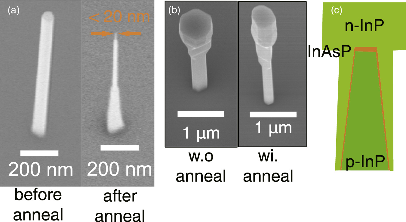
Fig. 1. (a) SEM image of InP NW before and after in situ annealing. (b) SEM image of InAsP NW formed with and without in situ annealing of InP NW. (c) Schematic cross-section of the heterostructure NW.
Download figure:
Standard image High-resolution imageAfter growth, NW-LEDs were fabricated using the standard process described in Refs. 30 and 34. Briefly, NWs were buried with benzocyclobutene (BCB), and the top portion of the NW was exposed to make contact between n-InP and indium tin oxide (ITO) electrodes. Vacuum-evaporated AuZn was used as the electrode on the back of a p-type substrate. NW-LEDs were characterized on-wafer using probes at RT or wired in a package after dicing for characterization at RT and LT. The current density was calculated by dividing the current by the area in which the NW array was formed (50. × 50 μm2). Low-temperature micro-PL (μ-PL) measurements using a HeNe laser as an excitation source were also performed on the as-grown NWs. The EL and PL from the sample were collected using microscope objectives and dispersed into a spectrometer equipped with a cooled InGaAs photodiode array photodetector.
3. Results and discussion
3.1. PL characterization
First, we present the results for low-temperature PL of a single NW. The PL results from the samples formed with and without annealing of the InP NW are compared and summarized in Fig. 2. In both NWs, we observed emission from InP at approximately 900 nm, and broad emission at approximately 1300 or 1200 nm originating from InAsP. In addition, we observed multiple sharp peaks at approximately 1389 nm (0.893 eV) in the sample without annealing, and at approximately 1515 nm (0.817 eV) in the sample formed with annealing. The linewidth of the peaks was 0.91 meV and 0.71 meV, respectively, for samples formed without and with annealing of InP NW. We attributed these sharp peaks to originating from QDs formed in the InP NWs. To confirm this hypothesis, we investigated the excitation intensity dependence of these emissions. The results for the sample formed with annealing are shown in Fig. 2(b). The peaks labeled as X and XX were resolved, and it was confirmed that peak X increased linearly with the excitation intensity, and XX increased proportionally to the square of the excitation intensity, as shown in Fig. 2(c). Similar results were obtained for the peak at approximately 1389 nm for the sample formed without annealing (data not shown). Thus, we conclude that the present results indicate the formation of an InAsP QD in the NWs, and X and XX correspond to the emission of excitons and biexcitons in the QDs, respectively.

Fig. 2. Results of low-temperature PL measurement. (a) Broad range PL spectra of samples formed with (blue line) and without (red) in situ annealing of InP NW, (b) excitation intensity dependence of the spectra at around 1520 nm of the sample with annealing, and (c) dependence of the integrated intensity on excitation power.
Download figure:
Standard image High-resolution imageIn the case of the sample formed without annealing, we believe that the QDs were formed by the fluctuation of the well width of the quantum well (QW) formed on top of the InP NW because the lateral size of the NW was not sufficiently narrow to provide lateral quantum confinement. The broad emission at higher energies is due to the QWs formed on the top of the NW. For a sample formed with annealing, a QD is likely to form at the tip of the InP NW if the tip of the InP NW is sufficiently narrow (∼20 nm), as shown in Fig. 1(b). However, because the annealed InP NWs were tapered, the growth of InAsP at the sidewall was also highly likely, which led to the formation of a QW at the sidewall of the InP NWs. In addition, QDs can be formed at the sidewall owing to the thickness fluctuation or alloy composition fluctuation of the InAsP on the NW sidewall. In other words, discrete localized states resembling QDs are formed in the sidewall QW. These parasitic QW and QDs are thought to be the origin of the emission at 1200 nm and relatively narrow peaks between 1200 and 1500 nm, respectively.
3.2. RT characterization of NW-LEDs
Figure 3 summarizes the results of the room-temperature characterization of the NW-LEDs formed with and without annealing the InP NWs. Considering the area and the pitch of the NW array (a = 3 μm), we estimated that approximately 300 NW were connected in parallel within the LED pattern (50 × 50 μm2) of the NW array. Although the leakage current under reverse bias was much larger than that expected in the ideal pn-junction diode, rectifying current–voltage (I–V) characteristics were confirmed, as shown in Fig. 3(a). We believe that the reverse leakage current was mainly due to the leakage current through the top and bottom electrodes, suggesting insufficient isolation between them. In fact, our recent reports on InP NW-LEDs 35,36) show that the amount of reverse leakage varies from sample to sample. The NW-LED fabrication process must be optimized to reduce the reverse leakage current. The analysis of the forward bias characteristics gave ideality factors n of 5.4 and 8.2, and series resistances Rs of 0.133 and 0.065 Ω cm2 for the samples with and without annealing, respectively. Large ideality factors indicate that the current through the pn-junction is dominated by the tunneling, as in the case of InP homojunction NW LEDs, 34) as discussed in the next section. In the EL spectra of Figs. 3(b) and 3(c), we confirmed a broadband emission including 1.0–1.6 μm (or 1.5 μm in samples with in situ annealing). Emissions longer than 1.6 μm were not confirmed owing to the cutoff of the detector. This emission wavelength range is on the longer wavelength side compared to the InAsP/InP NW-LEDs in our previous study, with the InAsP layer formed under pAsH3 = 4%. 30) Thus, we conclude that emissions covering telecom bands using InP-based heterostructured NWs can be achieved by introducing an InAsP layer with a larger As alloy composition. Figure 3(d) shows the current density J versus integrated light intensity L (J–L) characteristics of the two samples, and both show that the integrated intensity increases nearly linearly with the current density. In this figure, the ratio η of L and the injection current I, which is a measure of the external quantum efficiency (EQE), 34) is also shown as a function J and is almost constant for both samples. Therefore, we conclude that efficient carrier injection into InAsP was achieved in the present heterostructured NW-LEDs at RT, and no significant carrier overflow was confirmed at the current injection level.

Fig. 3. Results of RT EL measurement of NW-LEDs formed with and without in situ annealing of InP NWs. (a) I–V characteristics, (b) EL spectra and its injection current dependence of the NW-LEDs formed without in situ annealing of InP NW, (c) EL spectra of the NW-LEDs formed with in situ annealing of InP NW. (d) Comparison of integrated intensity L and η = L/I, which is equivalent to EQE, of the two samples. Left inset of (a) shows the linear plot of the I–V characteristics, and right inset of (b) shows the vidicon camera image of the NW-LED without current injection and under current injection.
Download figure:
Standard image High-resolution imageThe spectra and their peaks were located at lower energies for samples formed with in situ annealing of InP compared to the sample formed without annealing. The EL spectra exhibited a blueshift when the injection current was increased in both samples. This is thought to be due to band filling. The blueshift due to band filling was larger in the samples formed with in situ annealing. These results suggest that the energy distribution of the density of states (DoS) in the InAsP layer is different between the two samples and that samples with annealing have a broader energy distribution in DoS. As described in the previous section, parasitic InAsP QWs are expected to be formed at the sidewalls of the NWs in the sample formed with annealing and are the origin of the EL emission in the telecom band.
3.3. Low-temperature characterization
Finally, we attempted the low-temperature characterization of the NW-LED. A heterostructured NW-LED using an NW array formed with in situ annealing of InP was used for this investigation. The pitch a of the array was 1 μm and approximately 2800 NWs were measured in parallel. The characterization results are shown in Fig. 4. Figure 4(a) shows optical microscopy image of the NW-LED and its emission images at RT and low temperature (LT, ∼9 K) taken with a vidicon camera at a forward bias voltage of 2 V. Uniform emissions were confirmed in this sample at both RT and LT. Figure 4(b) compares the J–V characteristics of an NW-LED at RT and LT on a semi-logarithmic scale. The ideality factor n and series resistance were calculated to be 3.88 and 0.024 Ω cm2 at RT. The current was more than two orders of magnitude smaller at LT than at RT; however, the slopes in the forward-bias regions were almost the same at both temperatures. This implies that the current is dominated by tunneling. 37) Figure 4(c) shows the LT EL spectra at different current densities together with the PL spectra. We obtained the emissions including the telecom band at LT for both EL and PL. It should be noted, however, that EL emissions longer than 1.4 μm were almost completely suppressed, whereas PL included a wavelength range from 1.4 to 1.6 μm. It is also clear that the emission exhibits a large blueshift with an increase in the injection current density. In Fig. 4(d), we compare the EL spectra at RT and LT at similar current injection levels. We can confirm the blueshift due to temperature, but the amount of blueshift (∼170 meV) is much larger than that expected from the temperature dependence of the band gap energy of InAsP (∼70 meV). The amount of blueshift at LT was much larger than that observed at RT. In Fig. 4(e), the integrated EL intensities L and η are plotted as a function of the current density J at RT and LT. The efficiency η is approximately 18 times larger at LT than at RT at the same injection level. This enhancement is due to the reduction in nonradiative recombination, but the value is much smaller than the ratio of the PL efficiency of the InAsP-related emission (ratio of the integrated PL intensity of the InAsP-related peak) between LT and RT (approximately 250). At RT, L is nearly proportional to J; thus η is nearly independent of the injection current, as shown in Fig. 2(e). However, at LT, L depends on J as L  J1.07, resulting in a monotonous increase in η with J. The reason for the slight superlinear dependence of L on J is not clear at present.

Fig. 4. Results of EL measurement at RT and LT for a NW-LED sample formed with in situ annealing of InP NW. (a) Optical microscopy and emission image of a NW-LED under measurement. A vidicon camera was used to take emission images. (b) I–V characteristics at room and low temperatures. (c) EL and PL spectra measured at low temperatures. (d) Comparison of EL spectra at two different current injection levels and at RT and LT. (e) Plot of integrated EL intensity L and efficiency η.
Download figure:
Standard image High-resolution imageAlthough emission above 1.4 μm was strongly suppressed in the LT EL, sharp lines attributable to emission from the QDs or discrete localized states were observed at LT at approximately 1.25 μm. The results are shown in Fig. 5. In this measurement, a spatial filter was inserted between the microscope objectives and spectrometer to increase the spatial resolution and limit the number of NWs to be detected in the EL spectrum. We can see narrow peaks at 1248.0 nm (unassigned), 1250. 4 nm (labeled as X), and 1252.0 nm (XX). The linewidth of the sharp peak labeled X was 0.36 meV at a very low injection level. The integrated intensity of peak X increased linearly with injection current I when the broad background emission was subtracted. Peak XX appeared at the higher-energy side of peak X and developed superlinearly with I. Note that the ratio of the peak heights of X and XX was different for I = 108 and 189 μA. The integrated intensity of the XX peak was proportional to I2. These EL results are analogous to the exciton and biexciton emissions in QD observed in PL measurements (Fig. 2) and in LED with self-assembled QD. 12) However, care must be taken that we measured multiple NWs with pn-junction in parallel and, because of possible nonuniformities between NWs, the current flowing in one NW may not be doubled when the total current is doubled. Nevertheless, we believe that the peaks X and XX originate from excitons and biexcitons in a QD, respectively, obtained by current injection. To unambiguously determine whether the intensity is proportional to I or I2 for excitons and biexcitons, the measurement of current through single NWs is required.

Fig. 5. LT EL spectra showing sharp lines at around 1250 nm measured with higher spatial resolution to detect EL from few NWs.
Download figure:
Standard image High-resolution image
3.4. Discussions
In the NW-LED investigated in this study, EL originating from the InAsP layer was obtained in the wavelength range of 1.2 ∼ 1.6 μm at RT. If we consider the difference of the band gap energy between RT and 0 K for InAs or InP is in the range of 63–70 meV, 38) the EL from the InAsP layer shows blueshift and is expected to be obtained in the wavelength range from 1.12 to 1.47 μm at LT. The low-temperature PL results in Fig. 3(c) also suggest the existence of an InAsP layer having band gap energy corresponding to 1.2 ∼ 1.6 μm wavelength range. However, the blueshift in the EL spectra was much larger when the temperature was varied. Furthermore, the amount of blueshift induced by current injection was larger at LT than at RT. As a result, emission in the wavelength range from 1.4 to 1.6 μm was strongly suppressed in the LT EL spectra. This resulted in the failure to observe emissions with narrow linewidth attributable to QDs or localized states in EL measurements at wavelengths longer than 1.4 μm.
The reason for the unexpectedly large blueshift caused by temperature and current injection is not clear at present, but we think it is related to the mechanism of carrier injection into the active InAsP layer. If the pn-junction is ideal, carrier injection from InP to InAsP expected to occur by diffusion and energy relaxation; however, carrier injection via tunneling is much more likely because the current–voltage characteristics in Fig. 4(b) indicate that the current through the pn-junction is dominated by tunneling. In our previous study, we observed radiative tunneling in homojunction InP NW-LEDs, 34) where the EL peak was located at qV and its height was proportional to exp(qV/ET). Here, q is the elementary charge, V is the forward bias voltage applied across the pn-junction, and ET is the characteristic energy of tunneling. 34,39,40) Our present results for the heterostructured NW-LEDs did not follow the characteristic features of radiative tunneling, but we speculate that the interplay of the two types of carrier injection may influence the shape of the EL spectra. It is also possible that the layer structure of the NW-LEDs results in an inefficient carrier injection. As shown in Fig. 1(e), the present NW-LED structure is a core–shell pn-junction and heterostructure, and electrodes are formed only in the upper part of the n-InP. Based on the SEM image shown in Fig. 1, the thicknesses of the InAsP and InP shell layers were estimated to be approximately 50 nm. Assuming a donor concentration of 1018 cm−3 and the surface state distribution modeled in Ref. 41, the width of the depletion layer from the sidewall is estimated to be approximately 20 nm. Although this implies that the shell layers are only partially depleted, the small effective thickness of the InP shell layer and its finite resistivity significantly limit the current path. If the current injected from the top n-InP layer does not spread sufficiently to the sidewall of the n-InP NWs, carrier injection into the InAsP layer at the sidewalls does not occur. In this case, an improvement in the fabrication process is required to form ITO electrodes on the sidewalls of the NWs by exposing the n-InP sidewalls. It is also necessary to form the desired QDs only at the tip of the InP NWs. Nevertheless, it is necessary to clarify the mechanism and pathway of carrier injection in heterostructure NW-LEDs in future studies.
4. Conclusions
We grew InP-based heterostructure NWs with a pn-junction and an InAsP active layer using selective-area metal-organic vapor phase epitaxy and demonstrated NW-LEDs operating in the telecom band. Although the emission from the InAsP QDs above 1.5 μm was observed by low-temperature photoluminescence measurement, sharp emission lines above 1.4 μm were not confirmed in the EL spectra under current injection. Although the mechanism was not clarified, it resulted from the large blueshift of the EL spectra upon current injection and the suppression of emission by current injection in the low-energy tail of the InAsP layer. Elucidation of the mechanism of current injection into the InAsP layer at low temperatures and further optimization of the layer structure and annealing conditions are required for current-driven single-photon sources using NWs.
Acknowledgments
The authors thank Prof. Kazuhisa Sueoka, Dr. Hironori Gamo, Ms. Yukari Tatsumi, and Mr. Masahiro Sasaki for experimental support. Part of this work was financially supported by a Grant-in-Aid for Scientific Research from the Japan Society for the Promotion of Science (JSPS) (Grant No. 17H03223). Part of this work was supported by the "Advanced Research Infrastructure for Materials and Nanotechnology in Japan (ARIM)" of the Ministry of Education, Culture, Sports, Science and Technology (MEXT), Grant No. JPMXP1222HK0082 (Hokkaido University).