
Full version of a presentation at the 51st Annual Meeting of the Microscopy Society of America, Cincinnati, August 1993.
D. McMullan, Cavendish Laboratory, University of Cambridge, UK.
Correspondence to: Dr D. McMullan, MP Group, Cavendish Laboratory, Madingley Road, Cambridge CB3 0HE,U.K.
Copyrighted and reprinted with the permission of SCANNING, and/or the Foundation for Advances of Medicine and Science (FAMS), Box 832, Mahwah, New Jersey 07430, USA.
Summary: This article gives an account of the origins of the scanning electron microscope (SEM) and traces its development up to 1965 when the first SEM was marketed by the Cambridge Instrument Company. The survey concentrates on the SEM, as distinct from the microanalytical electron probe instruments that were also being developed during this period.
Key words: scanning electron microscopy; imaging of solid samples, history.
Contents: Introduction
Invention of scanning
Scanning optical microscopy
Charged particle beams
Electron beam scanner
Von Ardenne's Scanning Electron Microscope
The RCA Scanning Electron Microscope
The Cambridge Scanning Electron Microscope
Other SEMs up to 1965
Electron Probe X-Ray Analysers
Conclusion
Acknowledgement
References
Figure captions
From the very beginning of electron microscopy the imaging of solid samples was an important goal, particularly as the methods for producing thin samples were only developed later. The first attempt was by Ruska (1933) with the sample surface normal to the viewing direction and illumination by an electron beam at grazing incidence to the surface; he obtained images of copper and gold surfaces but at a magnification of only 10X. A few years later he made a second attempt (Ruska and Muller 1940) with the same geometry and with only marginally better results. Von Borries (1940) was much more successful with his grazing incidence method in the transmission electron microscope (TEM) where the sample surface is at a few degrees both to the viewing direction and to the illuminating beam. This is still an important technique.
A breakthrough in the microscopic imaging of surface topography in the TEM was the introduction of replicas by Mahl (1941) and these set the standard for the next 25 years although they were tedious to make and could be subject to serious artefacts. An example is shown in fig. 1.
During the 1930s a very different way of imaging solid samples, scanning electron microscopy, was invented by Knoll (1935) for the study of the targets of television camera tubes. Two years later von Ardenne (1938a,b) built an electron microscope with a highly demagnified probe for scanning transmission electron microscopy (STEM) and also tried it as an SEM. And soon afterwards Zworykin et al (1942a) developed a dedicated SEM. The beginning of the general use of the (SEM) can be accurately dated to 1965 when the Cambridge Instrument Company in the U.K. marketed their Stereoscan 1 SEM (to be followed about 6 months later by JEOL in Japan). This was thirty years after the initial developments in Germany and the U.S.A., but it was the research project started in 1948 by Oatley at the Cambridge University Engineering Department that led directly to the Stereoscan (Oatley 1982).
The purpose of this article is to trace the development of the SEM up to the sale of the first commercial SEMs in 1965. Incidentally it will be seen that many of the ideas put forward by the early workers were well ahead of their time, becoming technologically practicable only much later. The development of microanalytical probe instruments is summarised only briefly.
The 1928 date in the title of this article is somewhat arbitrary and it was chosen because the first mention of scanning applied to microscopy was made in that year. But it is relevant to start nearly 100 years earlier with the invention by Alexander Bain, a Scottish clockmaker, of the principle of dissecting an image by scanning, and the granting of a British patent (Bain 1843) for the first fax machine (McMullan 1990). At the transmitter, a stylus mounted on a pendulum contacts the surface of metal type forming the message, thus closing an electrical circuit, and at the receiver a similar stylus, also on a pendulum, records electrochemically on dampened paper. Following each swing of the pendulums, the type and the recording paper are lowered one line; means for starting the pendulums swinging simultaneously and synchronising magnetically are described in the patent.
The first proposal in print for applying scanning to microscopy was made by Synge (1928), in Dublin. This was for a scanned optical microscope and his aim was to overcome the Abbe limit on resolution by what is now called "near-field microscopy", that is the production of a very small light probe by collimation through an aperture smaller than the wavelength of the light.
Synge was a scientific dilettante who had original ideas in several scientific fields but did not attempt to put them into practice (McMullan 1990). However he considered some of the problems that would be encountered with a scanning microscope and he proposed the use of piezo-electric actuators (Synge 1932), as are now used with great success in the scanning tunneling microscope and other probe instruments, including of course the near-field optical microscope itself. He envisaged fast scanning of the sample so that a visible image could be displayed on a phosphor screen, and he also pointed out the possibility of contrast expansion to enhance the image from a low contrast sample - probably the first mention of image processing by electronic means (as distinct from photographic).
A proposal for using an electron beam in a scanning instrument was described by Stintzing (1929 a,b), of Giessen University, in German patents. These patents were concerned with the automatic detection, sizing and counting of particles using a light beam, or for those of sub-light microscopic size, a beam of electrons. Focussing of electrons was at that date unknown to him, as to most others, and he proposed obtaining a small diameter probe by crossed slits. The sample was to be mechanically scanned in the case of a light beam, and electric or magnetic fields would deflect an electron beam. Suitable detectors were to be used to detect the transmitted beam which would have been attenuated by absorption or scattering. The output was to be recorded on a chart recorder so that the linear dimension of a particle would be given by the width of a deflection, and the thickness by the amplitude; the production of a two-dimensional image was not suggested. Stintzing did not apparently attempt the construction of this instrument and there are no drawings accompanying the patent specification.
Knoll, the co-inventor of the TEM with Ruska, was the first to publish images from solid samples obtained by scanning an electron beam (Knoll 1935). In 1932, very soon after the building of the first TEM at the Berlin Technische Hochschule, he moved to the Telefunken Company to work on television camera tubes. There he developed an electron beam scanner for studying the targets of these tubes. The sample was mounted at one end of a sealed-off glass tube (fig. 2) and an electron gun at the other; the accelerating potential was in the range 500 - 4000 V. The electron beam was focussed on the surface of the sample and scanned by deflection coils in a raster of 200 lines and 50 frames/s. The current collected by the sample (the difference of the incident and secondary emitted currents) was amplified by a thermionic tube amplifier and intensity-modulated a cathode-ray tube which was scanned by deflection coils connected in series with those on the electron-beam scanner. By changing the ratio of the scan amplitudes the magnification could be varied, a principle which had been demonstrated by Zworykin (1934, 1942a) on an optical microscope fitted with a TV camera. Knoll used unity magnification most of the time but he could increase it to about 10 times before the resolution was limited by the diameter of the scanning probe.
This apparatus had virtually all the features of an SEM but, surprisingly in view of his earlier work on the TEM, Knoll did not use additional electron lenses to reduce the size of the probe below 100 micron; however the resolution he obtained was entirely adequate for his purpose. The beam current was relatively high, of the order of microamps, and therefore thermionic tubes could be used to amplify the signal current in spite of the fast scan rate.
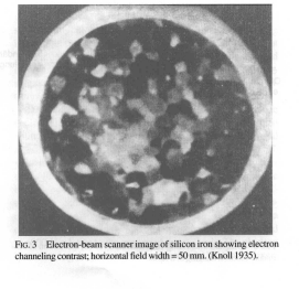
Similar images were no doubt produced by others working on the development of TV cameras in the 1930s, but Knoll was the only one at the time who looked at samples other than camera tube targets, for example silicon iron (fig. 3), and he also elucidated the contrast mechanisms: secondary electron coefficient and topography.

The images he observed were true secondary electron images because the electron gun and sample were enclosed in the highly evacuated and baked glass envelope and there was therefore little or no contamination of the surface. It is only comparatively recently that UHV SEMs have been available which can work in this imaging regime.
Knoll continued using his electron beam scanner (which he named "der Elektronenabtaster") for a number of purposes including the study of oxide layers on metals (Knoll 1941).
The first scanning electron microscope with a sub-micron probe was developed by von Ardenne, a private consultant who had his own laboratory in Berlin, over the very short period of about 2 years; he also had had experience in the development of TV camera tubes (von Ardenne 1985). In 1936 he was contracted by Siemens and Halske AG to investigate the possibility of using a scanned electron probe to avoid the effects of objective lens chromatic aberration with thick samples in TEM. In the course of this work he laid the foundations of electron probe microscopy by making and publishing (von Ardenne 1938a,b) a detailed analysis of the design and performance of probe-forming electron optics using magnetic lenses. The analysis covered the limitations on probe diameter due to lens aberrations and the calculation of the current in the probe. He also showed how detectors should be placed for bright-field and dark-field STEM and for imaging a solid sample in an SEM, and considered the effects of beam and amplifier noise on imaging.
In order to fulfil the Siemens contract he built the first STEM and demonstrated the formation of probes down to 4 nm diameter. But in the short time available he was limited to employing existing technology, and because there was no suitable low-noise electronic detector available, he used photographic film to record the image.
 Consequently there was no immediately visible image. A schematic of the microscope column is shown in fig. 4: a demagnified image of the crossover of the electron gun was focussed on the sample by two magnetic lenses, and X-Y deflection coils were mounted just above the second of these. Immediately below the sample was a drum around which was wrapped the photographic film.The image was recorded by rotating the drum and simultaneously moving it laterally by means of a screw while the currents in the deflection coils were controlled by potentiometers mechanically coupled to the drum mechanism. The intensity of the beam was very low (about 10*E-13 A) and it was necessary to record the image over a period of about 20 min. Since the image was not visible until the film had been developed, focussing could only be accomplished indirectly by using the stationary probe to produce a shadow image of a small area of the sample on a single-crystal ZnS screen which was observed through an optical microscope and prism system. The recordings were inferior to those from the TEM that was being constructed by Ruska and von Borries at Siemens, and the hoped-for advantages of STEM with thick samples were not fulfilled.He spent a short time trying to use the instrument in the SEM mode on bulk samples, but only low resolution images could be obtained because of the detector problem: the sample current was amplified by thermionic tubes and a large probe current was needed. He did not publish any images.


In total, von Ardenne worked for less than two years on scanning electron microscopy before concentrating on the development of his universal TEM (von Ardenne 1985); and then, with the start of the war, on building a cyclotron and isotope separators for nuclear energy projects. If he had been able to continue, there is little doubt that he would have built an efficient SEM within a year or two: this is evidenced by a patent (von Ardenne 1937) which included a proposal for double-deflection scanning, two papers (von Ardenne 1938a,b), and a book (von Ardenne 1940). Two of the chapters in the book were on scanning microscopy and were based on the 1938 papers but included additional material relating to imaging the surfaces of solid samples. Most importantly he proposed a detector using an electron multiplier with beryllium copper dynodes (see fig. 5) which could be opened to the atmosphere and work efficiently under poor vacuum conditions. Measurements of the secondary emitting ratio of beryllium copper and its stability when exposed to the atmosphere were first reported only in 1942 by I. Matthes of the AEG Research Institute in Berlin, but von Ardenne was probably aware of this research a year or two before. In his book he also discussed the interaction between the beam electrons and the sample and suggested that back-scattering would cause a loss of resolution, illustrating this with a diagram which has a quite modern look (fig. 6). He argued that the incident beam electrons produce secondary electrons at or near the surface from an area approximately equal to the beam diameter and give a high resolution image ("nutzbare Strahlung"); the beam electrons then penetrate the sample and a proportion of them are back-scattered and reach the surface where they produce further secondaries. These two signals are now generally referred to as SE-I and SE-II respectively (Drescher et al. 1970, Peters 1982). The back-scattered electrons are emitted from an area of diameter comparable with the penetration depth, and the secondaries they produce ("schadliche Strahlung") may impair the resolution (however he did not consider the case of a sample with small inclusions below the surface). He concluded that good resolution might be obtained either with a very low energy beam (1 keV), or with one having a high energy (50 keV). In the first case the back- scattered electrons would emerge from an area of the surface little larger than the incident beam and the resolution would be unaffected. On the other hand with a 50-keV beam the secondary electrons would be produced by the back-scattered electrons over a very much larger area; moreover they would be evenly distributed so that their main effect would be to increase the background (reduce the contrast) rather than to affect the resolution.
Von Ardenne's scanning microscope was destroyed in an air raid on Berlin in 1944, and after the war he did not resume his work in electron microscopy but researched in other fields: first in Russia and from 1955 in Dresden, which was then in the D.D.R.. Additional information about von Ardenne's scientific work has been given in his autobiography (von Ardenne (1972)) and by McMullan (1988).
The RCA Scanning Electron Microscope
 Meanwhile in America, Zworykin, Director of Research at the RCA Camden NJ laboratories, had in 1938 initiated a development programme on SEM (Zworykin et al. 1942a) which continued until about 1942. This work was done in parallel with the development of a TEM and by the same staff, in particular Hillier, Ramberg, Vance and Snyder as well as Zworykin himself.
Although Zworykin had every microscope paper from Germany translated as soon as it was received (Reisner 1989) he was apparently not influenced by von Ardenne's work on the SEM. Instead he started by, in effect, repeating Knoll's beam scanner experiments using a "Monoscope"; this was a pattern-generating cathode-ray tube which had been developed by RCA for television use (Burnett 1938) and was very similar to Knoll's apparatus. He then built an SEM based on the Monoscope but with two magnetic lenses to produce a very small focussed probe, and a demountable vacuum system so that the sample could be changed (Zworykin et al. 1942a). The scan rate was the U.S TV standard, 441 lines and 30 frames/s, and the signal was amplified by a thermionic tube video amplifier. For a signal-to-noise ratio of 10 the signal current had to be 3 x 10*E-8 A which could only be reached if the probe diameter was about 1 micron.
He next tried to obtain a high current in a smaller probe by the use of a field emission gun with a single-crystal tungsten point (Zworykin et al. 1942a), presumably based on experience with the point projection microscope that had been built in the RCA Laboratories by Morton and Ramberg (1939). To obtain a sufficiently high vacuum he had to return to having the gun and the sample in a glass envelope which was baked and sealed-off. A single magnetic lens was used, and fleeting images were obtained at 8000X magnification with scanning at TV rate and a thermionic tube amplifier. Stable images could no doubt have been achieved but at that time a practical microscope would not have resulted because demountable UHV techniques did not exist.
To overcome the noise problem Zworykin therefore decided to build a SEM with an efficient electron detector and a slow scan. The detector was the combination of phosphor and photomultiplier that Everhart and Thornley used nearly twenty years later in an improved form. In order to bring the secondary electrons to it he designed an electrostatic immersion lens which retarded the beam electrons and accelerated the secondaries. Figure 7 shows the final electron optical arrangement: electrostatic lenses were used to produce a demagnified image of the source on the sample which was held at +800 V relative to the grounded gun cathode. The electron beam leaving the gun was accelerated to 10 keV in the intervening electron optics. The accelerated secondary electrons diverged as they passed through the 4th electrostatic lens and hit the phosphor screen with an energy of 9.2 keV.
 In the first instrument the scanning was done by moving the sample relative to the beam electro-mechanically using loudspeaker voice coils and later hydraulic actuators; it was only in the final version that magnetic scanning of the beam was employed. The scan time was fixed at 10 min by the facsimile recorder which was used for image recording and which also controlled the microscope scans. There was no provision for a faster scan and the production of a visible image on a TV monitor; this seems strange remembering Zworykin's TV background, but it may have been because the signal bandwidth was limited by the decay time of the phosphor as was found in later work at Cambridge (McMullan 1952). The focus setting was found by maximising the high frequency components in the video waveform observed on an oscilloscope, a method which was originally proposed by von Ardenne (1938b).
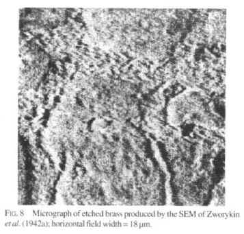
Although the intention was to produce contrast by differences in the secondary emission ratio of the surface constituents, and the incident beam energy of 800 eV was chosen with this in mind, contamination of the surface in the rather poor vacuum prevented meaningful compositional contrast being obtained. Actually, all of Zworykin's published micrographs were of etched or abraded samples, and contrast was topographic (Zworykin et al. 1942b), for example etched brass (fig. 8). The quality of the recorded images was rather disappointing, and together with the lack of a visible image must have been a factor in RCA deciding to discontinue the project. But another reason was undoubtedly the excellent results that were, as mentioned in the Introduction, being obtained with replicas in TEMs. In the event all available technical effort had to be directed to the highly successful RCA EMB TEM, which was then coming into production (Reisner 1989).
The Cambridge Scanning Electron Microscopes
 Apart from a theoretical analysis of resolving power by a French author (Brachet 1946), no other work on the SEM had been reported by 1948. The feeling among electron microscopists appeared to be that it was not worth further consideration in view of the apparent failure of the RCA SEM - if such an experienced team were unsuccessful it was very unlikely that anyone else could produce an effective instrument; a notable exception to this general opinion was Gabor (1945). It was then that Charles Oatley at the Engineering Laboratories of the University of Cambridge decided that another look at the SEM might be worthwhile, although, as he has related, "several experts expressed the view that this [the construction of an SEM] would be a complete waste of time" (Oatley et al 1985). He has explained at some length the reasons that brought him to this decision but the main technological ones were that "Zworykin and his collaborators had shown that the scanning principle was basically sound and could give useful resolution in the examination of solid surfaces" and "improvements in electronic techniques and components had resulted from work during the war" (Oatley 1982). He was also of the opinion that the RCA detector had a low efficiency and only a small proportion of the secondaries were reaching it, with the result that the images were noisy in spite of the long recording time. Independently of von Ardenne he proposed an electron multiplier with beryllium-copper electrodes (Allen 1947) having been promised one by Baxter of the Cavendish Laboratory who was building multipliers of this type (Baxter 1949).
I was selected by Oatley to build an SEM as a Ph.D. project, a challenging task because electron microscopy was a completely new subject for everyone in the laboratory although I had had some experience in the radar and television industries including the development and manufacture of cathode-ray tubes. I first completed a 40 keV electrostatically focussed TEM which had been begun by another PhD student, K.F. Sander; he had abandoned it at an early stage and had changed the subject of his research project to electron trajectory plotting (Sander 1951). I converted it an STEM, and then to an SEM, by the addition of scan coils, the electron multiplier detector and a long persistence cathode-ray tube monitor (McMullan 1952).
It was still far from clear how Zworykin's results might be improved on. A higher incident beam energy could be expected to be beneficial but it was not clear how image contrast would be formed. Bruining and de Boer (1938) had shown that the secondary emission from a surface is critically dependent on the vacuum conditions and it was plain that a high enough vacuum would not be achieved for there to be meaningful secondary-electron compositional contrast from a polished sample.
As mentioned in the introduction, images of surfaces had been obtained at grazing incidence and viewing direction (2 deg) in the TEM by von Borries (1940), and others, and it seemed probable that similar images could be produced in the SEM. I therefore mounted a sample of etched aluminum at a rather larger angle (30 deg, because the back-scattered electrons did not have to be focussed) and was rewarded by the now commonplace three-dimensional appearance that is the hall-mark of SEM images; this is a consequence of the large depth of focus. One of the first images, of etched aluminum, is shown in fig. 9: (a) the direct view image, 1.8-s frame period, and (b) a 5- min recording. The beam energy was 16 keV and the resolution about 50 nm, limited by astigmatism in the objective lens and insufficient magnetic shielding.
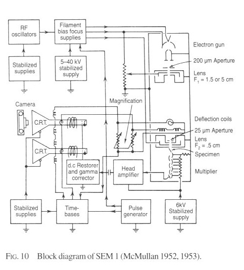 A block diagram of the SEM is shown in fig. 10 (McMullan 1953) and a cross-section of the column in fig. 11. There was a relatively fast- scan long-persistence cathode-ray tube display (405 lines, 1.9 fields/s interlaced) and a slow scan (5 min) display for photographic recording; other features included a non-linear amplifier for gamma control, and beam blanking for D.C. restoration. Double-deflection scanning coils were added later. The most important differences between this instrument and Zworykin's were the much higher incident beam energy at the sample (15-20 keV) and the contrast was produced mainly by scattered electrons. The mechanism of contrast formation was investigated and was shown to be topographic. No attempt was made to collect low- energy secondaries and in fact I thought that they would be detrimental because of the inevitable contamination on the surface of the sample. I overlooked the increase in signal that is obtained from the low energy secondaries.
 I realised that there was another advantage in using a high energy scanning beam: this was that in principle atomic number contrast was possible using backscattered electrons. An experimental curve of emission ratio (for 20-keV primaries) versus atomic number had recently been published by Palluel (1947), but an attempt at obtaining atomic number contrast failed; some years later Wells (1957) was more successful. The obvious disadvantage of high beam energies was that the resolution was limited by penetration of the primary electrons and I suggested low-loss electron imaging (LLE) to minimise this, but was not able to implement it. One other contrast mechanism that I tried was cathodoluminescence and was able to demonstrate that phosphors which had too long a decay constant to be used to produce a 1.9-s frame time image with a Zworykin-type detector were completely satisfactory when excited at a high current density by a focussed probe.
figure 12 is a photograph of the SEM taken in 1953 shortly before K.C.A. Smith assumed responsibility for it and turned this first instrument into an SEM which could produce images comparable with those from modern microscopes. He introduced improvements including a stigmator and a tilting sample stage, and he increased the efficiency of the detection system by moving the electron multiplier nearer the sample so that low-energy secondary electrons could be collected, thus increasing the signal current. He also showed that metallised insulating samples could be imaged, and he examined a wide variety of samples including thermal decomposition of silver azide, germanium point-contact rectifiers, and fungus spores in water vapour in an environmental cell (Smith and Oatley 1955, Smith 1956).

The electron multiplier was a bulky device and in 1956 Oatley suggested that an aluminised short-decay-time plastic scintillator plus photomultiplier might be worthwhile investigating. Smith first used this combination to detect high-energy back-scattered electrons and later two more of Oatley's students, Everhart and Thornley, developed it as the secondary electron detector that bears their names (Everhart and Thornley 1960).
Further SEMs were built in the Engineering Department: SEM 2 (Wells 1957), SEM 3 (Smith 1961), SEM 4 (Stewart 1962), and SEM 5 (Pease and Nixon 1965). All were used on a wide variety of samples, and for the development of new techniques. Other important instrumental advances made by Oatley's group during the remainder of the 1950s and to 1965 included: atomic number contrast (Wells 1957); stereomicroscopy (Wells 1960); voltage contrast (Oatley and Everhart 1957); low-voltage (1 kV) SEM (Thornley 1961); high temperature (1200 degK) imaging of thermionic cathodes in a SEM (Ahmed 1962); high resolution (10 nm) SEM (Pease and Nixon 1965); etching of surfaces in a SEM by ion bombardment (Stewart 1962); ion etching and microfabrication in SEM (Broers 1965); microelectronics in SEM (Chang and Nixon 1956). In addition EBIC imaging was first demonstrated by Wells et al. (1963), but not in Cambridge. Most of this work is described in papers by Oatley (1982) and Oatley et al. (1965, 1985).
Smith completed the SEM 3 (fig. 13) in 1958; this was the first magnetically focussed SEM (Smith 1959, 1961). The lower section of the column below the table consisted of a modified Metropolitan Vickers (later AEI) type EM4 TEM (Page 1954) and contained the electron gun, condenser lens, transmission sample stage, objective lens, and double pole-piece projector lens. For scanning operation, the transmission objective and double projector were used together in various combinations and powers according to the spot diameter required to provide the first stage of spot demagnification. Immediately above the table there was a section of the column containing the scanning coils and the objective lens which was of the pin-hole type (Liebmann 1955) with three adjustable apertures. There was a tilting sample stage and the secondary electron detector was of the Everhart-Thornley type.
 The SEM 3, which was the first fully engineered SEM, had been commissioned by Thiesmayer and Atack of the Canadian Pulp and Paper Research Institute and was used for examining wood fibres in their Ottawa laboratories: this was the earliest industrial use of an SEM on a daily basis. They were among the very few who at that time saw the great potential of SEM (Atack and Smith 1956): although Oatley's group had produced and published high quality micrographs, from many different samples, there was still considerable resistance to SEM. Over several years Oatley expended much effort in trying to persuade electron microscope manufacturers to market an SEM (Jervis 1971, Oatley 1982) but he was finally successful only in 1962 when the Cambridge Instrument Company decided to go ahead with the production of the "Stereoscan" (fig 14) which was based on the instruments developed by Oatley's group (Stewart and Snelling 1965). The prototype went to the Dupont Chemical Corporation in the USA in 1964 and in the following year the first 2 production models were sold to Thornton at the University of North Wales and to Sikorski at Leeds University in the UK, and the 3rd to Pfefferkorn at Munster University in Germany. The Japanese firm JEOL marketed their JSM-1 SEM about 6 months later.
SEM developments in other laboratories up to 1965, as evidenced in scientific publications, included the following. An SEM was built in France by Bernard and Davoine (1957) at the National Institute of Applied Science in Lyon: it had a probe size of the order of 1 micron and was used over a period of years mainly for cathodoluminescence studies. In the UK, AEI, then a major TEM manufacturer, developed an SEM but did not proceed after the first instrument, sold in 1959, turned out to be unsatisfactory (Jervis 1971). In the early 1960s, at the Westinghouse Laboratories in Pittsburgh, Wells, Everhart, Matta and others built an advanced SEM for semiconductor studies and microfabrication and demonstrated EBIC imaging (Wells et al. 1965). And in the USSR there was an SEM at Moscow University from about 1960 (Kushnir et al.). There were other groups, especially in Japan, who did not publish at the time.
Electron Probe X-ray Analysers
Although peripheral to the subject of this article, the salient events in the development of the electron probe x-ray microanalyser will now be briefly summarised. Originally proposed by Hillier in 1947, a static probe instrument was developed by Castaing and Guinier in Paris in 1949 and marketed by the French firm Cameca in 1956. Cosslett at the Cavendish Laboratory in Cambridge started a research programme in 1953 which led two years later to a scanning microanalyser built by Duncumb (Cosslett and Duncumb 1956). This was further developed at the Tube Investments Research laboratories near Cambridge (Duncumb and Melford 1960) and was marketed as the "Microscan" by the Cambridge Instrument Company in 1960. In the U.S.A. microanalysers were developed by Birks and Brooks (1957) among others. Firms in several countries were marketing microanalysers by 1965; the probe sizes were generally around 1 micron and electron imaging was only an adjunct. A few years later SEMs were being equipped with the newly introduced energy-dispersive silicon diode spectrometers and x- ray microanalysis on SEM samples is now routine.
This article has described how the development of the scanning electron microscope from concept to the marketing of a commercial instrument in 1965 took 30 years. The foundations were laid in the 1930s by Max Knoll (b. 1897, d. 1969) who first obtained scanned electron images from the surface of a solid, and by Manfred von Ardenne (b. 1906) who established the principles underlying the SEM including the formation of the electron probe and its deflection, the positioning of the detector, and ways of amplifying the very small signal current. The technology necessary for the realisation of his ideas was only just becoming available and because of the very short time he had for the development of an SEM he was unable to put them into practice.
Vladimir K. Zworykin (b. 1889, d. 1982) and his team at the RCA Research Laboratories built an SEM which had several important original features but its performance was not adequate to persuade electron microscopists of its usefulness.
The idea was revived in 1948 by Charles Oatley (b. 1904) at the Cambridge University Engineering Department and over the next 15 years a succession of his research students built 5 SEMs of increasingly improved performance culminating in the production of a commercial instrument by the Cambridge Instrument Company.
The contributions of Knoll, von Ardenne, Zworykin, and Oatley to the genesis of the scanning electron microscope should be recognised by the many thousands of microscopists who today use this instrument in virtually every field of scientific research.
The author would like to thank Dr Oliver Wells for his helpful comments on an earlier version of this article.
Ahmed H: Studies on high current density thermionic cathodes. PhD Dissertation, Cambridge University (1962)
Allen JS: An improved electron multiplier particle counter. Rev Sci Instrum 19, 739-749 (1947)
Atack D, Smith KCA: The scanning electron microscope - A new tool in fibre technology. Pulp Pap Mag Can 1, 245-251 (1956)
Bain A: Electric time pieces and telegraphs. British patent no 9745, filed 27 May 1843
Baxter AS: Detection and analysis of low energy disintegration particles. PhD Dissertation, Cambridge University (1949)
Bernard R, Davoine F: The scanning electron microscope. Ann Univ Lyon Sci Sect B[3] 10, 78-86 (1957).
Birks LS, Brooks EJ: Electron probe x-ray microanalyser. Rev Sci Instrum 28, 709-712 (1957)
Brachet C: Note sur le pouvoir séparateur du microscope électronique à balayage. Bull Assoc Tech Marit Aeronaut no 45, 369-378 (1946)
Broers AN: Selective ion beam etching in the scanning electron microscope. PhD Dissertation, Cambridge University (1965)
Bruining H, deBoer J.H.: Secondary emission. Physica (Amsterdam) 5-30, 17 (1938)
Burnett CE: The Monoscope. RCA Review 2, 414-420 (1938)
Castaing R, Guinier A: Application des sondes électroniques à analyse métallographique. Proc Conf Electron Microsc, Delft pp 60-63 (1949)
Chang THP, Nixon WC: Electron beam machining of silicon observed with SEM (Abstract). J Appl Phys 37, 3937 (1966)
Cosslett VE, Duncumb P: Micro-analysis by a flying-spot x-ray method. Nature 177, 1172-1173 (1956)
Drescher H, Reimer L, Seidel H: Rückstreukoeffizient und Sekundärelektronen-Ausbeute von 10-100 keV-Elektronen und Beziehungen zur Raster-Elektronenmikroskopie. Z angew Phys 29 331 (1970)
Duncumb P, Melford DA: Design considerations of an x-ray scanning microanalyser used mainly for metallurgical applications. Proc 2nd Int Symp X-ray Microsc Microanalysis, Stockholm pp 358-367 (1960)
Everhart TE, Thornley RFM: Wide-band detector for micro-microampere low-energy electron currents. J Sci Inst 37, 246-248 (1960)
Gabor D: The Electron Microscope. Hulton Press, London (1945)
Hillier J: Electron probe analysis employing x-ray spectrography. US Patent No 2,418,029 (1947)
Jervis P: Innovation in electron-optical instruments - two British case histories. Research Policy 1, 174-207 (1971)
Knoll M: Aufladepotentiel und Sekundäremission elektronenbestrahlter Körper. Z tech Phys 16, 467-475 (1935)
Knoll M: Nachweiss aufgewachsener Oxydschichten des Eisens mit dem Elektronenabtaster. Phys Z 42, 120-122 (1941)
Kushnir YuM, Fetisov DV, Raspletin KK: Scanning electron microscope and x-ray microanalyser. Bull Acad Sci USSR Phys Ser (Engl Transl) 25, 709-714 (1961)
Liebmann G: The magnetic pinhole electron lens. Proc Phys Soc London Ser B 68 682-685 (1955)
Mahl H: Über das plastische Abdruckverfahren zur übermicroskopische Untersuchung von Oberflächen. Z tech Phys 22, 33-38 (1941)
Matthes I: Untersuchungen über die Sekundärelektronenemission von verschieden Legierungen. Z tech Phys 22, 232-236 (1942)
McMullan D: Investigations relating to the design of electron microscopes. PhD Dissertation, Cambridge University (1952)
McMullan D: An improved scanning electron microscope for opaque specimens. Proc Inst Electr Engrs 100, Part II, 245-259 (1953)
McMullan, D: Von Ardenne and the scanning electron microscope. Proc Roy Microsc Soc 23, 283-288 (1988)
McMullan D: The prehistory of scanned image microscopy Part 1: scanned optical microscopes. Proc Roy Microsc Soc 25, 127-131 (1990)
Morton GA, Ramberg EG: Point projector electron microscope. Phys Rev 56, 705 (1939)
Oatley CW: The early history of the scanning electron microscope. J Appl Phys 53, R1-R13 (1982)
Oatley CW, Everhart TE: The examination of p-n junctions in the scanning electron microscope. J Electron 2, 568-570 (1957)
Oatley CW, Nixon WC, Pease RFW: Scanning electron microscopy. Adv Electronics Electron Phys 21, 181-247 (1965)
Oatley CW, McMullan D, Smith KCA: The development of the scanning electron microscope. In The Beginnings of Electron Microscopy (PW Hawkes ed) Adv Electronics Electron Phys Suppl 16, 443-482 (1985)
Page RS: A compact consoe-type electron microscope. J Sci Instrum 31, 200-205 (1954)
Palluel P: Composante rediffusee du rayonnement electronique secondaire des metaux. C R Acad Sci 224, 1492-1494 (1947)
Pease RFW, Nixon WC: High resolution scanning electron microscopy. J Sci Inst 42, 81-85 (1965)
Peters K-R: Generation, collection and properties of an SE-1 enriched signal suitable for high resolution SEM on bulk specimens. In Electron Beam Interactions with Solids SEM (Inc), Chicago, pp 363-372 (1982)
Reisner JH: An early history of the electron microscope in the United States. In Adv Electronics Electron Phys 73, 134-231 (1989)
Ruska E: Die elektronenmikroskopische Abbildung elektronenbestrahlter Oberflächen. Z Phys 83, 492-497 (1933)
Ruska E, Muller HO: Über Fortschritte bei der Abbildung elektronenbestrahlter Oberflächen. Z Phys 116, 366-369 (1940)
Sander KF: An automatic electron trajectory tracer and contributions to the design of an electrostatic electron microscope. PhD Dissertation, Cambridge University (1951)
Smith KCA: The scanning electron microscope and its fields of application. PhD Dissertation, Cambridge University (1956)
Smith KCA: Scanning electron microscopy in pulp and paper research. Pulp Pap Mag Can Tech Sect 60, T366-T371 (1959)
Smith KCA: A versatile scanning electron microscope. Proc European Conf Electron Microsc, Delft, pp 177-180 (1961)
Smith KCA, Oatley, CW: The scanning electron microscope and its fields of application Br J Appl Phys 6, 391-399 (1955)
Stewart ADG, Snelling MA: A new scanning electron microscope. Proc 3rd European Conf Electron Microsc, Prague, pp 55-56 (1965)
Stewart ADG: Investigation of the topography of ion-bombarded surfaces with a scanning electron microscope. Proc 5th Internat Conf Electron Microsc, Philadelphia, pp D12-13 (1962)
Stintzing H: Verfahren und Einrichtung zum automatischen Nachweiss, Messung und Zählung von Einzellteilchen beliebiger Art, Form und Grösse. German patent No 485155 (1929a)
Stintzing H: Einrichtung zum automatischen Nachweiss, Messung und Zählung von Einzellteilchen beliebiger Art, Form und Grösse nach Patent 485155, insbesondere zur Erzeugung sehr enger Strahlenbündel. German patent No 485156 (1929b)
Synge EH: A suggested method for extending microscopic resolution into the ultra-microscopic region. Phil Mag 6, 356-362 (1928)
Synge EH: An application of piezo-electricity to microscopy. Phil Mag 13, 297-300 (1932)
Thornley RFM: Recent developments in scanning electron microscopy. Proc. European Conf. Electron Microsc., Delft, pp. 173-176 (1961)
von Ardenne M: Das Elektronen-Rastermikroskop. Theoretische Grundlagen. Z Phys 109, 553-572 (1938a)
von Ardenne M: Das Elektronen-Rastermikroskop. Praktische Ausführung. Z tech Phys 19, 407-416 (1938b)
von Ardenne M: Improvements in electron microscopes. British patent no 511204, convention date (Germany) 18 Feb 1937 von Ardenne M: Elektronen-Übermikroskopie. Springer Verlag, Berlin (1940); Edwards Brothers Inc, Ann Arbor (1943)
von Ardenne M: Ein glücklische Leben für Technik und Forschung Kinder Verlag, Munich and Zurich (1972)
von Ardenne M: On the history of scanning electron microscopy, of the electron microprobe, and of early contributions to transmission electron microscopy. In The Beginnings of Electron Microscopy (PW Hawkes ed) Adv Electronics Electron Phys Suppl 16, 1-21 (1985)
von Borries B: Sublichtmikroskopische Auflösungen bei der Abbildung von Oberflächen um Übermikroskop. Z Phys 116, 370-378 (1940)
Wells OC: The construction of a scanning electron microscope and its application to the study of fibres. PhD Dissertation, Cambridge University (1957)
Wells OC: Correction of errors in electron stereomicroscopy. Brit J Appl Phys 11, 119-201 (1960)
Wells OC, Everhart TE, Matta RK: Automatic positioning of device electrodes using the scanning electron microscope. IEEE Trans Electron Dev ED-12, 556-563 (1965)
Zworykin VA: Electric Microscope. 1st Congresso Internazionale di Electroradio-biologia Atti 1, pp 672-686 (1934)
Zworykin VA, Hillier J, Snyder RL: A scanning electron microscope. ASTM Bull 117, 15-23 (1942a)
Zworykin VA, Hillier J, Snyder RL: A scanning electron microscope (Abstract). Proc Inst Radio Engrs 30, 255 (1942b)
1. TEM image of an early oxide replica of etched aluminum (Mahl 1941); horizontal field width = 9 micron.
2. Schematic diagram of Knoll's (1935) electron-beam scanner.
3. Electron-beam scanner image of silicon iron showing electron channeling contrast; horizontal field width = 50 mm. (Knoll 1935= ).
4. Cross-section of the column of von Ardenne's (1938b) STEM. ("Strahlerzeugungssystem" = electron gun; "Verkleinerungsoptik" = reducing lens; "magnet. Ablenksystem" = deflection coils; "Objekt" = sample; "Registriertrommel" = film recording drum).
5. Electron multiplier with beryllium copper dynodes proposed by von Ardenne (1940) as a secondary electron detector for an SEM. The drawing shows the first three stages of the multiplier and its position relative to the objective lens and sample.
6. Diagram illustrating von Ardenne's (1940) discussion of secondary electron imaging of a surface.
7. The electron optics of the SEM built by Zworykin et al. (1942a).
8. Micrograph of etched brass produced by the SEM of Zworykin et al. (1942a); horizontal field width = 18 micron.
9. One of the first images (etched aluminum) produced with the Cambridge SEM 1 microscope. Angle of incidence of 16-keV electrons 25 deg.: (a) visible image, 0.95 frames/s, beam current 1.5 x 10*E-10A, horizontal field width = 37 micron; (b) 5 min recording, 10*E-13A, horizontal field width = 15 micron
10. Block diagram of SEM 1. (McMullan 1952, 1953).
11. Cross-section of the column of SEM 1. (McMullan 1952, 1953).
12. Photograph of SEM 1 taken in 1953.
13. The first magnetically focussed scanning electron microscope (SEM3) built by K.C.A. Smith for the Pulp and Paper Research Instituteof Canada (Smith 1959, 1961).
14. The prototype of the first Stereoscan SEM, supplied by theCambridge Instrument Company to the duPont Company, U.S.A.(Stewart and Snelling 1965). Courtesy of Leica Ltd.
Copyrighted and reprinted with the permission of SCANNING, and/or the Foundation for Advances of Medicine and Science (FAMS), Box 832, Mahwah, New Jersey 07430, USA