


Transmission electron microscopy has functioned for decades as a platform for in situ observation of materials and processes with high spatial resolution. Yet, the dynamics often remain elusive, as they unfold too fast to discern at these small spatial scales under traditional imaging conditions. Simply shortening the exposure time in hopes of capturing the action has limitations, as the number of electrons will eventually be reduced to the point where noise overtakes the signal in the image. Pulsed electron sources with high instantaneous current have successfully shortened exposure times (thus increasing the temporal resolution) by about six orders of magnitude over conventional sources while providing the necessary signal-to-noise ratio for dynamic imaging. We describe here the development of this new class of microscope and the principles of its operation, with examples of its application to problems in materials science.
I. INTRODUCTION
The first in situ experiments in the transmission electron microscope (TEM) were performed shortly after it was routinely deployed to investigate microstructure in thin metal films. The context for these observations has been reviewed by Hirsch1,2 and the actual observations of moving dislocations were reported in 1956.3 These observations of dislocations gliding on their crystallographic slip planes removed the remaining doubts about the role of dislocations in plastic deformation that were lingering at the time. The breakthrough enabling the observations was the ability to make artifact free specimens of metals sufficiently thin for electron transparency. The Cambridge group used ion milling to thin aluminum, as first developed by Castaing,4 while an independently developed investigation of dislocations at the time by Bollman used electropolishing.5 This early discovery highlights the importance of well-controlled specimen geometry in electron microscopic investigations6 and is a theme that returns often, particularly with in situ observations.
Even with carefully designed specimens, not all aspects of in situ observations can be clearly interpreted. An interesting example that served as an inspirational case study for improving the time resolution of TEM was the work of Minor et al.7 In this work, aluminum specimens were shaped into prisms, and the triangular cross section tip of the prism that was thin enough for electron transparency was used for observations. A sharp diamond indenter was brought into contact with the tip of the prism by a fine piezo drive and the load was measured as a function of displacement. Previous reports on nanoindentation of metal surfaces had presented load-displacement curves that at a critical load would have a sudden, unstable displacement take place. The interpretation of this behavior was that at a critical load under the indenter, the nucleation barrier for dislocation formation at the surface or the activation of dislocation sources was overcome, and a sudden burst of dislocation activity was responsible for the displacement jump of the indenter. However, the in situ observations showed that dislocation activity preceded the displacement burst and actually occurred throughout the loading portion of the indentation. While this observation was important and necessary for the reinterpretation of the metal nanoindentation results, some aspect of the observations remained unclear. Specifically, the images were recorded on a video recording device that captured an image every 24th of a second (42 ms). It was evident to the researchers that dislocations would form, propagate, interact with other dislocations or obstacles, and come to rest positions all in the span between image acquisitions. It became clear that for a full interpretation of these experiments that a much faster means of acquiring the images was needed.
In this review of time resolved electron microscopy for in situ materials science experiments, we will start with the pioneering work of O. Bostanjoglo at the Technical University of Berlin (TU Berlin). The TU Berlin work explored several different approaches to high time resolution microscopy, culminating in an approach we call “single shot” microscopy. Lawrence Livermore National Laboratory (LLNL) chose the single shot approach as being the most relevant to materials science investigations and its further development is covered in Sec. III, including its extension to “Movie Mode”. Finally, several examples of the technique applied to materials science studies are presented.
II. BACKGROUND
A. Stroboscopic microscopy
One of the first approaches to achieving high time resolution on the TEM was the use of a stroboscopic approach. This approach is taken because the exposure time for acquiring an image on a microscope cannot be arbitrarily shortened. The issue is the level of current generated by the electron source in a TEM. While the standard electron source will generate several μA of emission, not all of these electrons are useable, and gun optics and apertures in the column reduce the current to typically several tens of nA at the specimen in the process of increasing the coherence of the illumination. As an example, if we consider a current of 10 nA, it is 6 × 10¹⁰ electrons per second. We have found as a practical matter that greater than 109 electrons are required to form an image with sufficient signal to noise ratio as to have interpretable contrast. Therefore, for this beam current, an exposure time of at least 16 ms is required to form an image. Of course, shorter exposure times could be produced by higher beam currents, however practical limitations are quickly reached, and achieving substantially sub ms exposure times is severely limited. However, if many short exposure images could be summed together, then the signal to noise ratio of the total could be improved to the needed level for interpretation. This approach then gives rise to the stroboscopic approach.
For a stroboscopic approach to be used on a dynamically evolving specimen, the phenomenon under study must be oscillatory such that it can be probed many times at the same instant in its cycle and the signal integrated over many cycles to build the signal to noise ratio to an acceptable level. One such cyclic phenomenon is the motion of magnetic domain walls under the influence of an oscillating magnetic field. Thus, stroboscopic imaging was first applied in Lorentz imaging mode.8,9 The periodic illumination of the specimen was achieved by blanking the beam from a conventional electron source with electrostatic deflection plates. This imaging mode was used to study resonance properties of single and coupled domain walls as a function of excitation frequency10–14 with direct observation of the wall motions.
Recent advances in the stroboscopic approach to time resolution have pushed into the fs regime by using short pulse laser technology to create the cyclic electron illumination.15–17 In this approach, a short laser pulse from a high repetition rate laser is split and one branch goes to the specimen while the other branch goes to the microscope photocathode emitter in the electron gun after being converted to the ultra-violet. Delay line optical paths vary the relative timing of the two branches. The branch brought to the specimen is used to pump the cyclic process of interest. The branch brought to the gun creates one to several emitted electrons within a precisely defined time window for each cycle. This pump-probe cycle is repeated for millions to billions of times to build the signal to noise in resultant diffraction or imaging data. This laser based stroboscopic microscopy has been used to study such cyclic processes as the elastic vibration of a cantilever,18 vibration of membranes,19,20 or—when combined with spectroscopy—transient electronic states.21
The stroboscopic approach is generally limited to studying processes that can be repeated cyclically and rapidly in exactly the same way for millions of times. The TEM in materials science is typically applied to characterizing microstructural features that control properties and determine performance. These features include dislocations, precipitates, grain boundaries, and phase boundaries. The motion of these features through a microstructure during processing or service is a thermodynamically lossy process. This interaction with thermal vibrations of the solid imparts a stochastic nature that prevents the evolution of these features from unfolding in exactly the same way twice. Thus, the further development of time resolved microscopy has focused on “single shot” techniques, in which all of the signal required to form an image or diffraction pattern is acquired in with a single time resolved pulse of electrons of extremely high instantaneous brightness.
B. Streaking the signal
Recognizing the limitations of the stroboscopic technique, the TU Berlin group implemented a technique to investigate single events such as phase transformations by monitoring total electron intensity in the microscope. The unscattered or small angle scattered electrons that form the transmitted beam in the electron microscope will, in most cases, undergo a change in intensity upon a change in the diffracting conditions in the specimen. Such changes can be induced by changes in crystal orientation or crystal structure due to a transformation. The change generally occurs by the change in the total number of electrons that undergo large angle scattering, for example by a diffraction condition. These large angle scattered electrons can then be blocked by the insertion of an aperture in the back focal plane of the objective lens. The transmitted electrons are then fed into an amplification system and finally an oscilloscope to record changes in intensity as a function of time. Specific locations on the specimen can be chosen by using a selected area aperture in diffraction mode or by condensing the beam in imaging mode. This technique has been used to study the crystallization kinetics of amorphous Si,22 Ge,23,24 and Fe-Ni alloys25 when rapidly heated by laser irradiation. While this method can study irreversible processes, it cannot take advantage of the most powerful aspect of the TEM, which is to acquire images at high spatial resolution. One approach to retaining imaging information with streaking across the detector is to take the signal from a slit across the image and deflect it across a 2D detector array. This was done with melting and vaporization transformations,26–28 however, the difficulty of data interpretation limits its applicability. The benefits of creating single shot time resolved images became apparent.
C. Single shot imaging
The strength of the electron microscope is its ability to acquire images at high spatial resolution. To capitalize on this strength, the first attempts to shorten the exposure time for image acquisition used a standard thermionic electron source and either pulsed the detector29–31 or used fast electrostatic deflection32,33 to create a pulsed electron beam. These approaches suffered from poor signal to noise ratio because of the limitations of the standard thermionic emission current. Producing higher instantaneous currents for much shorter time periods, that is to say, making high intensity pulses of electrons, was found to be a more productive path.
A key step to producing short pulses of electrons is the introduction of an optical path into the gun area of the electron microscope to transport a pulse of laser light to an emitter. The electron guns of microscopes are typically tight spaces that constrain the choices for the optical path, dictating some level of engineering inside the vacuum of the microscope, such as the introduction of a laser window and a mirror. The first approach taken was to use the laser pulse as a heat source to raise the localized temperature of a spot on the emitter to the point where appreciable electron emission occurs.34,35 One advantage of this approach is that the emitter need not be changed from the usual tungsten hairpin used in the gun. The emitter can then be used in the usual thermionic mode (sometimes called the continuous wave (CW) mode in this context) for alignment of the microscope optics and positioning of the specimen prior to the time resolved experiment. In pulsed mode, the emitter is preheated to a point below appreciable emission and the laser pulse then heats a small spot on the emitter surface. The laser pulse is typically generated by a Nd:YAG based laser, with a duration of around 10 ns. The specific duration of the laser pulse depends greatly on the design of the laser and offers an area of great flexibility in the design of the system. In the initial work being discussed here,34,35 the single pulse duration was 15 ns and was frequency doubled to 532 nm with energies per pulse of several 10 s of μJ. The microscope used by this group in most of their investigations was a Siemens Elmiscope 1A, which allowed for a relatively short path length between the final focusing optic of the laser optical system and a sufficient convergence angle to achieve a 40 μm spot diameter on the emitter. Electron emission is confined to the area of the emitter heated by the laser pulse and a smaller emission region results in better coherence of the electron illumination. The physics of electron emission in this case is multifaceted35 and leads to a complex temporal structure to the electron pulse. Nonetheless, this pulsed electron source achieves the goal of creating an electron beam that is about 50 times the brightness of a conventional thermionic source,36 albeit for a short duration of around 20 ns.
In experiments using pulsed-laser-generated thermal emission of electrons, a second laser may be directed onto the specimen to initiate the process under study. The relative timing of the two laser pulses determines the time of the experimental observation. The approach has been used to study melting and resolidification of thin films of pure Fe and pure Ti36 and the intermixing and reaction of Al and Ni to form intermetallic phases.37 In the melting and solidification studies, the melt pool motion and solidification times were measured, as well as the identification of the first solid phases formed in these allotropic elements. Nanostructured mixtures of elemental Al and Ni were discovered to have self-propagating reaction fronts sustained by the highly exothermic formation of intermetallic phases.38 The mixtures of Al and Ni made for the investigations in Ref. 37 did not sustain such self propagating fronts but did undergo reaction when heated with a pulsed laser. The authors were able to use time resolved diffraction analysis to track phase formation in thin films with compositions of 3Al:1Ni and 1Al:3Ni.
Another application of the pulsed laser thermionic electron source that the group at TU Berlin investigated was a reflection electron microscope to investigation surface reactions.39 These authors reported an investigation of the ablation of GaAs from intense pulse laser irradiation.
Further evolution of the technique was driven by the desire to increase the signal to noise ratio by increasing the number of electrons in a single pulse, while nominally keeping the pulse duration the same. This goal was advanced by using photoemission rather than thermal emission to produce electrons at the cathode. Efficient photoemission is created by single photon absorption providing sufficient energy to an electron so that it can escape the surface and be accelerated away in the applied electric field. The group in TU Berlin approached this technical objective by using the fourth harmonic of the Nd:YAG for the cathode laser (266 nm wavelength). Several cathode target materials were tried and Zr or ZrC materials with a rough surface on a Re wire produced by powder sintering were found to give the best performance.40 These materials have low work functions and the rough surface enhances emission relative to a flat surface by a mechanism that may include curvature-enhanced fields or simply increased surface area in the illuminated region. A pulsed photoemission source was also implemented on a mirror electron microscope for near surface characterization of materials.41
The pulsed photoemission source was used to study melt dynamics in a Ni alloy.42,43 This microscope was equipped with rapidly switched electrostatic deflection plates that allowed it to collect three images on a single CCD camera exposure, allowing dynamics to be measured. A series of studies was performed on laser ablation of materials,44–47 mostly metals, and acceleration as high as 109 g was measured for particles ejected from the laser spot. These measurements demonstrated the capability of multiframe imaging system that allows position determination at precisely defined times to make highly accurate measurements of speed and acceleration. This instrument was also used to study phase transformations, specifically the hcp to bcc transition at elevated temperature in Ti.48,49
The development and evolution of nanosecond electron microscopes at TU Berlin has been covered in greater detail in two previous review articles by the researchers themselves.50,51
III. INSTRUMENTATION AND CAPABILITIES
The effort to build a single-shot nanosecond-imaging dynamic transmission electron microscope (DTEM) at Lawrence Livermore National Laboratory started in 2003. The decision on the base microscope upon which to build the instrument was taken in consideration of the substantial unknowns at the time about the extent of instrument modifications that would be required. A microscope with a reputation for robust operation, but that was considerably more advanced than what was used by TU Berlin group, was chosen. The base microscope at TU Berlin had always been a Siemens Elmiskop 1A (introduced in 1958). The microscope used at LLNL is a JEOL JEM-2000FX (introduced in 1984). One of the main differences in the newer microscope is substantially reduced optical aberrations and chromatic aberration. As mentioned already, the technique is constrained by the brightness of the electron source and short duration of the electron pulse. The requirement to improve the signal to noise ratio drives the operation of the microscope to larger convergence angles of the illumination to use as many electrons as possible generated at the source, but this concomitantly reduces the spatial coherence of the illumination. The energy spread of the electrons from the photocathode is also expected to be greater than from a traditional thermionic source. For both of these reasons, the lower aberrations of the newer microscope gives substantially improved images over what had been possible previously.
A. The cathode laser system
The choice of the pulsed laser system to drive photoemission at the microscope cathode is just as important a consideration as the choice of microscope itself. Early on in the design of the system, the use of the fifth harmonic was chosen, initially of a Neodymium-doped yttrium lithium fluoride (Nd:YLF) system (1054 nm fundamental) and subsequently, a Neodymium-doped yttrium aluminum garnet (Nd:YAG) system (1064 nm fundamental), giving wavelengths of 211 nm and 213 nm, respectively. This photon energy allowed the use of a simple (and commercially available) photocathode that consists of a Ta disk of 0.8 mm welded to the apex of a Ta wire bent into a hairpin shape spanning two electrodes. The increase in photon energy with respect to that used at TU Berlin (fourth harmonic 266 nm) has an order of magnitude increase in the photoemission quantum efficiency for Ta52 and thus obviated the need for cathode target material development. The Ta disk cathode brings the advantage that it is robust with respect to pulsed laser irradiation and will have a long service life due to the high melting point of the Ta. The emitter can also be used in the traditional thermionic mode by simple joule heating of the Ta disk by passing the usual current through the hairpin wire, allowing the microscope to be operated in the normal CW mode for alignment and experiment set up procedures.
Introducing the laser optical path into the gun area of the microscope required modifications to the electron optical column. These modifications will depend on the particular model of microscope being used, but the objective will be the same, which is to bring the laser pulse to the photocathode without the light optical elements required to do so interfering with the path of the electrons into the microscope column. With the advent of commercially available systems, these modifications may become more standardized in the future. Bringing the laser light into the vacuum system of the microscope requires a window that is transparent at 213 nm. These windows are commonly available and are typically fused silica, but they provide little attenuation of the x-rays generated within the column. When making this modification, great care is required to reestablish x-ray shielding to limit operator exposure primarily during CW operation. With the model of microscope used here, access to the gun was only possible from below, with the optical path following the electron column in the reverse direction up to the photoemitter. A short column section was inserted below the accelerator and above the condenser lens system that contains a window and a mounted mirror to direct the laser path up to the emitter (see Ref. 53 for more details). In turn, this mirror contains a through hole aligned with the electron optical path of the column to allow the emitted electrons through. The first results from this configuration of the instrument were reported in Ref. 54.
Careful measurements of the emitted charge as a function of laser energy per pulse showed that the number of electrons collected at the image plane of the microscope were two orders of magnitude less than predicted by considering the quantum efficiency of the photoemission process.53 These measurements revealed that the apertures in the microscope were blocking many of the emitted electrons. The solution to this problem revealed that the aperture in the mirror was the main source of the pulse attenuation and a more substantial modification to the electron optical column was required.55,56 For this modification, a weak lens was added to the condenser lens system and was dubbed the “C0” lens because it is above the C1 lens. This lens coupled with an added drift section of the column acts to couple the electron source through the hole in the mirror and into the column of the microscope with much greater efficiency and with minimal additional aberrations while the source is generating an instantaneous current of greater than 10 mA.
The first cathode laser system fitted to the DTEM was based on Nd:YLF amplification, and it delivered a single pulse at 10 Hz frequency. A shutter was used to select one pulse to perform a given experiment. The subsequent laser system, alluded to above with Nd:YAG amplification, is much more flexible and capable of generating a train of pulses that can be used to generate multiple images of a single evolving event in the specimen. It has been dubbed the Movie Mode laser for this reason. This laser system has been most thoroughly described in Ref. 57. The flexibility of this system is such that it can achieve a flat top pulse in time and in space on the cathode. The spatial flat top is achieved by illuminating an aperture with spatially even illumination and then relay imaging that aperture to the cathode location. A temporally flat top is achieved through pulse shaping technology. A continuous wave laser generates the seed of laser light that is fed into an acousto-optical modulator that carves out a programmed intensity as a function of time profile. The programmability of the system allows the waveform intensity to be essentially arbitrary as a function of time, and indeed, these systems are referred to as arbitrary waveform generators. The waveform can be a single pulse of varying intensity that has a user defined duration or it can be a train of multiple pulses with arbitrarily defined durations and spacing in time. The flat top temporal profile of the final pulse at the cathode requires that the decreasing gain in the amplification system as amplification proceeds is compensated for by supplying a higher intensity in the seed. This even illumination of the cathode in both time and space allows for the greatest total emission of electrons by the minimization of screening from Childs law effects.
B. The specimen drive laser
In the papers cited from the TU Berlin work and most of the LLNL work, the phenomena studied by in situ observation are initiated by a pulsed laser. In most cases, the laser pulse was in the ns regime, however, the TU Berlin group did compare ns to fs pulse response in materials.58 In the ns regime, the laser pulse can be regarded simply as a heating source because the energy is deposited in local thermodynamic equilibrium (electron temperature and ion temperature remain equilibrated). However, the heating rate is much higher than other means of heating. For example, a temperature rise of 1000 K in 10 ns translates to a heating rate of 1011 K/s. The laser pulse is typically focused to a spot on the specimen. In the LLNL DTEM, it is approximately 135 μm in diameter at full-width half maximum intensity (FWHM). In addition, the TEM specimen is thin, so there is only a small quantity of material to heat and the laser pulse can be of modest energy, typically only a few μJ per pulse.
The photon energy is also an important consideration. The nature of the specimen and the wavelength of the photons will determine how much energy is deposited in the irradiated spot. For example, a Ge specimen is highly transparent to the fundamental wavelength of approximately 1 μm, but it will readily absorb in the frequency-doubled wavelength of 532 nm. Therefore, the specimen laser on the DTEM has the flexibility to use the fundamental, doubled, or tripled wavelength. The amount of laser energy absorbed will determine the rise in temperature, so knowing the absorbing characteristics of the specimen is necessary for an estimation of the temperature rise. Ex situ measurements of laser energy reflection and transmission in an ellipsometer are useful tools in making these estimations. In addition, an in situ measurement of the laser energy required to reach the melting point of the specimen can provide a one point calibration for calculating the temperature during an experiment.
C. Recording images
Operating the microscope in a pulsed mode means that the time resolution of the experiment is determined by the pulse duration. There are no requirements on the time resolution of the detector. Hence, standardly available electron microscope cameras based on a scintillator fiber optically coupled to a CCD detector are used to record the images and diffraction patterns (DP). The detector is simply initiated at a specified time to begin accumulating signal, the duration is set to a time typical of an electron microscope exposure (∼1 s), and during this time, the pulse of electrons lands on the detector. The detector is read out afterwards and the image stored. However, pulse duration cannot be arbitrarily shortened to improve the time resolution because space charge effects will cause the image to blur below a certain level.59
Recording multiple images that comprise a movie is only slightly more complicated. The movie consists of typically nine frames that are arranged as a 3 × 3 array on the camera. The camera is acquiring only one image with patches of the detector area being the individual frames of the temporally evolving process imaged in the experiment. The individual electron pulses are steered onto these different patches by an orthogonal pair of electrostatic deflection plates. The time required to stabilize the voltage applied to the plates determines the minimum time between frames of the movie. The voltages needed for sufficient deflection are a few hundred volts for a position of the plates just under the last crossover of the microscope column. With commercially available voltage supplies, the minimum time between frames for the LLNL DTEM is 50 ns. This time could potentially be shortened with custom designed power supplies.
D. Control system and user interface
Integration of the various elements of the microscope is essential for coordinating their function relative to a specific time. A master timing reference must be established in order for timed trigger pulses to be sent to the various components of the instruments at predetermined times. The most effective way to bring all these various aspects of the instrument together for the user is with integrating control software such as LabView.
E. In situ stages
As part of the collaboration between the DTEM group at LLNL, the Johns Hopkins University, and NIST, instrumentation developments have recently enabled simultaneous nanocalorimetry and DTEM experiments.60 The experimental setup consists of the DTEM, a custom-built in situ TEM holder, a TEM-compatible nanocalorimeter chip, and a data acquisition system. By synchronizing the nanocalorimeter operation with the DTEM cathode laser system, pulsed electron images or diffraction patterns may be captured at any time during the heating cycle of the nanocalorimeter. This system enables simultaneous thermal and microstructural characterizations for heating rates from ∼103 up to 105 K/s. The time-resolved diffraction pattern aids the microstructural analysis of reactions, which is essential to nanocalorimeter experiments, and provides an opportunity to characterize reactions that are dependent on high heating rates in situ.
IV. MATERIALS SCIENCE EXAMPLES
A. Phase change materials (PCMs)
Chalcogenide-based PCMs are widely used in optical recording media and are important in the development of resistance-based non-volatile electronic memory. Phase change materials have two properties that make them technologically important: (1) the amorphous and crystalline phases have distinct differences in their optical and electronic properties and (2) they may be switched between phases rapidly and repeatedly through the application of heat pulses. For memory applications, it must be possible to switch between the amorphous and crystalline phases in nanoseconds. Heating may be achieved by laser- or current-pulses, but in either case, crystallization of the amorphous phase is the slower, data-rate-limiting process compared to the crystalline-to-amorphous melt-quench process, thus the crystallization kinetics are of especial interest in PCMs. Crystallization kinetics at the nanosecond time scale are especially relevant to memory applications.
Optical measurements during laser-crystallization offer the time resolution needed to track the fraction of material crystallized, but do not yield crystallographic information nor the microstructural information necessary to quantify the nucleation rate or crystal growth front velocity. The temporal resolution of conventional in situ TEM is orders of magnitude too slow to resolve growing crystalline grains during laser-induced phase transformations. Pulsed TEM has been used for time resolved studies crystallization of amorphous PCMs, including Ge-Te alloys24,61–65 and Ge2Sb2Te566 and has developed to the point where the temporal and spatial resolution is adequate to track the development of individual growing crystalline grains during laser crystallization and morphological changes.64,65,67
1. Crystallization of amorphous Ge-Te alloys
In the 1980s, Bostanjoglo and coworkers used a pulsed thermionic TEM to study the electron-pulsed-induced crystallization of amorphous Ge0.6Te0.424 and Ge0.8Te0.261 and laser-induced crystallization of amorphous Ge0.8Te0.2.62,63 In these early studies, phase transitions were detected as changes in the bright-field (BF) image intensity, which were detected by scintillator, multiplier, and storage oscilloscopes with a resolution of 3 ns in specimen areas >0.3 μm diameter.
The Ge-Te system forms a line compound at the 50%–50% composition and crystallization of these Ge-rich alloys was accompanied by phase separation. Electron-pulse-crystallized Ge-Te alloy films consisted polycrystalline GeTe and Ge phases in the center of the heated area, surrounded by large radially elongated crystals with some remaining amorphous material, in turn surrounded by amorphous GeTe with some crystalline grains. Crystals at the center of the heated area started to grow after a delay of several microseconds, but once initiated, the submicron area defined by the field-limiting aperture crystallized in nanoseconds. The crystal growth rate of electron-pulsed crystallized Ge0.6Te0.424 was estimated to be up to 1 m/s. Growth velocities of the different textures in electron-pulsed crystallized Ge0.8Te0.2 was estimated to range from 0.3 to 10 m/s.61 For amorphous Ge0.8Te0.2 crystallized by nanosecond laser pulses,62 four different phases were observed to grow with delays 1–20 μs after the heating laser pulse and with estimated growth rates as high as 6 m/s. The delay of the start of crystallization may have been caused by superheating of the alloys (requiring the specimen to cool before it could occur) or by diffusion-limited phase segregation. However, interpretation of changes in BF intensity was limited by the complexity introduced by the phase separations and by other factors that changed the BF intensity such as local thickness changes that developed during heating and buckling of the film caused by volume changes during crystallization.
Bostanjoglo and Thomsenschmidt63 later used double-frame pulsed TEM to image the transformations in amorphous Ge0.8Te0.2 films induced by laser-heating with exposure times ≥10 ns and variable delay times. Two sets of double-frame images were shown for two transformations induced by laser pulse. The image resolution was low, limiting the interpretation of the image contrast. A blotchy network of light and dark areas coarsened during the laser heating. The changes in image contrast were attributed to changes in film thickness, as confirmed by post-mortem characterization. Thus, the morphological development of the Ge0.8Te0.2 films was imaged, but the amorphous-to-crystalline transition itself remained obscure.
The superior spatial resolution of the DTEM at LLNL later allowed Santala et al. to image the amorphous-to-crystalline transition during laser-induced crystallization of amorphous stoichiometric GeTe.64,65 The 1:1 stoichiometric alloy crystallizes rapidly because no phase separation occurs and long-range diffusion does not limit the process. Stoichiometric GeTe is an attractive PCM for both high temperature and non-volatile RAM applications because of its high crystallization temperature.
Single-shot DTEM was first used to image crystallization in amorphous GeTe64 induced by 12 ns, 4.2–4.3 μJ laser pulses with a 135 μJ 1/e2 diameter. For the laser energies used, crystallization progressed initially at the highest rate in an annulus ∼15–25 nm from the center of the laser spot and proceeded inward and outward from the annulus. The nucleation rate was lower in the central region, than in the surrounding region, because the higher temperature diminished the driving force for nucleation. In a series of single shot experiments, 15-ns images of the central region were taken 300–900 ns after the specimen laser pulse (Figure 1). Individual growing grains were clearly imaged, but due to the highly stochastic nature of the nucleation events and the considerable incubation time for crystallization of as-deposited amorphous PCMs, the series does not provide a very continuous view of the nucleation and growth process.

Bright-field 15-ns single-shot DTEM images taken with different time delays after initiation of laser crystallization in amorphous GeTe. Since nucleation is highly stochastic and PCMs can have considerable incubation times before nucleation, the series of single-shot images does not form a full, continuous view of the process. Reprinted with permission from Santala et al., Phys. Status Solidi B 249(10), 1907–1913 (2012). Copyright 2012 WILEY-VCH Verlag GmbH & Co. KGaA, Weinheim and John Wiley & Sons, Inc.
Bright-field 15-ns single-shot DTEM images taken with different time delays after initiation of laser crystallization in amorphous GeTe. Since nucleation is highly stochastic and PCMs can have considerable incubation times before nucleation, the series of single-shot images does not form a full, continuous view of the process. Reprinted with permission from Santala et al., Phys. Status Solidi B 249(10), 1907–1913 (2012). Copyright 2012 WILEY-VCH Verlag GmbH & Co. KGaA, Weinheim and John Wiley & Sons, Inc.
The outward growth of the crystalline region was also imaged, 1400 ns after the heating laser pulse (Figure 2). The time-resolved image shows a compact front of small grains (<200 μm) ∼20 μm from the outside edge of the crystalline spot. The grain size remained similar to the edges of the crystalline region. Localized enhancement of nucleation along the front suggested a feedback mechanism caused by the heat released from the enthalpy of transformation. A rough estimate of nucleation rates during laser annealing was made using time resolved images for the time scale of crystallization and an estimate the density of nuclei taken from the grain size from post mortem images. The nucleation rate was estimated to be ∼10−4 μm−2 s−1 near the shot center to ∼10−7 μm−2 s−1 near the shot edge.
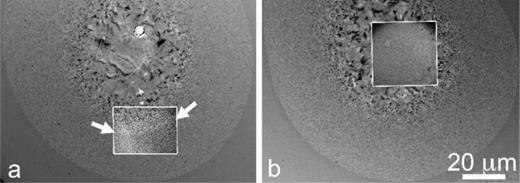
Conventional TEM images taken after crystallization with 4.2 mJ laser shots with 15-ns DTEM images during crystallization inset. The inset in (a) was taken 1400 ns after the pump laser pulse. The position of the crystallization front at 1400 ns is indicated by arrows. The box in (b) shows nucleation and inward growth of crystalline regions 500 ns after the heating laser pulse. Reprinted with permission from Santala et al., Phys. Status Solidi B 249(10), 1907–1913 (2012). Copyright 2012 WILEY-VCH Verlag GmbH & Co. KGaA, Weinheim and John Wiley & Sons, Inc.
Conventional TEM images taken after crystallization with 4.2 mJ laser shots with 15-ns DTEM images during crystallization inset. The inset in (a) was taken 1400 ns after the pump laser pulse. The position of the crystallization front at 1400 ns is indicated by arrows. The box in (b) shows nucleation and inward growth of crystalline regions 500 ns after the heating laser pulse. Reprinted with permission from Santala et al., Phys. Status Solidi B 249(10), 1907–1913 (2012). Copyright 2012 WILEY-VCH Verlag GmbH & Co. KGaA, Weinheim and John Wiley & Sons, Inc.
Crystal growth rates of amorphous PCMs cannot be accurately determined from single-shot DTEM, even if the image quality is high, because time of nucleation of each individual grain is unknown. A single image can give a lower bound on the growth rate assuming no incubation period occurred. The development of Movie Mode DTEM at LLNL with nine-frame pulsed TEM imaging has made accurate measurement of growth rates during laser crystallization possible. Such measurements have been made during laser crystallization of allowed the crystallization of amorphous GeTe.65 Nine-frame movies of each initiated reaction were generated from a series of nine 17.5-ns electron pulses. Precise growth rates were determined by tracking the position of crystallization fronts in each frame of the nine-frame movie. Figure 3 shows two image series during crystal growth at the center of the laser-affected areas. Although the same laser energy was used, the details of the crystallization process unfolded differently in each case. For the laser energy used, the growth rate initial exceeded 3 m/s with a slight drop in rate as time progresses.

Growth of crystalline regions (yellow) into amorphous GeTe (blue) in two nine-image series of 17.5-ns electron pulses after 4.7 μJ laser shots. The time in each frame is relative to the peak specimen laser intensity. Reprinted with permission from Appl. Phys. Lett. 102(17), 174105 (2013). Copyright 2013 AIP Publishing LLC.
Growth of crystalline regions (yellow) into amorphous GeTe (blue) in two nine-image series of 17.5-ns electron pulses after 4.7 μJ laser shots. The time in each frame is relative to the peak specimen laser intensity. Reprinted with permission from Appl. Phys. Lett. 102(17), 174105 (2013). Copyright 2013 AIP Publishing LLC.
The DTEM growth rate measurements were connected specimen temperature by simulating the temperature profile caused by laser heating. Temperature profiles were developed using finite element analysis modeling of laser-specimen interactions and heat flow. The simulated temperatures allowed the DTEM measurements to be placed in the context with low temperature isothermal measurements using a classical growth rate model. A calculated growth rate of a crystalline grain in a thin amorphous GeTe film is plotted in Figure 4 along with published growth rate data for GeTe from conventional microscopy experiments. Growth is limited at high temperature by the diminishing thermodynamic driving force and at lower temperatures by diminishing atomic diffusivity. Based on the observed reduction in growth rate and the expected local increase in temperature due to the enthalpy of crystallization, it was determined that the DTEM observations were made in temperature range where an increase in temperature of >100 K leads to a only small reduction in growth rate and where crystal growth is near its maximum rate (bold segment in Figure 4). Previously, growth rates had been measured with conventional optical microscopy and TEM over only a small temperature range where crystal growth is many orders of magnitude lower.
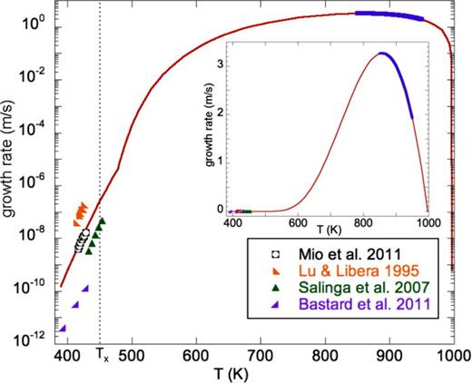
Crystal growth rate vs. temperature for amorphous GeTe thin films with data points from conventional microscopy experiments plotted with calculated rates (thin, red solid line) Growth rates measured with DTEM fall in the bold region where a drop in rate is expected due to a temperature increase caused by heat of devitrification released. The inset is plotted on a linear scale to emphasize the high temperature region. Reprinted with permission from Appl. Phys. Lett. 102(17), 174105 (2013). Copyright 2013 AIP Publishing LLC.
Crystal growth rate vs. temperature for amorphous GeTe thin films with data points from conventional microscopy experiments plotted with calculated rates (thin, red solid line) Growth rates measured with DTEM fall in the bold region where a drop in rate is expected due to a temperature increase caused by heat of devitrification released. The inset is plotted on a linear scale to emphasize the high temperature region. Reprinted with permission from Appl. Phys. Lett. 102(17), 174105 (2013). Copyright 2013 AIP Publishing LLC.
The comparison results of the single-shot versus multi-frame mode-mode DTEM imaging is a clear illustration of how important the multi-frame imaging capabilities will be in continuing research with PCMs and other materials systems. Further multi-frame DTEM research will build a more complete understanding of crystallization kinetics of GeTe and other PCMs.
2. Crystallization of amorphous Ge2Sb2Te5
Ge2Sb2Te5 is an important PCMs that has very wide use in optical memory devices. Because of its technological importance, it has been the subject of numerous theoretical and experimental studies, but application of pulsed TEM has been fairly limited to date. This may be attributed to the high nucleation rate Ge2Sb2Te5 which results in a very fine-grained structure during laser annealing at very high temperature approaching the melting point. The small grain size has to date limited imaging of the grains during growth; however, single-shot DTEM in diffraction mode has been used to study laser crystallization of as-deposited amorphous Ge2Sb2Te5. Santala et al.66 used the DTEM to follow the crystallographic changes during driven laser-induced crystallization. Laser-induced formation of meta-stable cubic Ge2Sb2Te5 from the amorphous phase can occur in as little as ∼10–100 ns in a device; however, during the in situ TEM experiment, crystallization neared completion in about 2 μs. This was attributed to the specimen geometry: the long crystallization time is due to low cooling rates in large thin, electron-transparent specimens as observed for GeTe.
To make the temporal temperature profile closer to that in a device, where cooling occurs on the nanosecond rather than microsecond scale, while maintaining electron transparency required for TEM, a wedge shape specimen was fabrication using microfabricated Si base onto which a metallization layer, the PCM, and a capping layer could be deposited.66 Rapid cooling was achieved as the specimen geometry enabled in situ melt-quenching of the specimen which requires cooling rates on the order of 1010 K/s. This was verified by conventional TEM, but the electron transparent region of the wedge was too small for pulsed TEM imaging at the time, due to limits in the electron signal.
B. Rapid solidification of metals and alloys
Solidification processing has long been utilized in the fabrication of metal and alloy components and systems for a broad spectrum of engineering applications. Rapid solidification, in particular, has been widely recognized as a viable processing route to obtain unique microstructures with potentially advantageous properties that cannot be obtained with conventional solidification processes.68,69 However, the fundamental challenge of understanding and controlling microstructure remains, and experimental techniques that can monitor microstructure evolution during solidification offer promise of improved microstructural control and properties. Direct experimental observations of metallic alloy solidification processes have been limited, and capturing the dynamics associated with rapid solidification has been further complicated by the high velocities of the transformation front, rendering microscopic experimental in situ imaging and characterization of the evolving microstructure and solidification front morphology extremely challenging. Hence, prior reports on microstructure evolution during rapid solidification have been based almost entirely on post-mortem analyses,70–72 and reports on solidification front velocities during rapid solidification usually represent averages for the complete liquid-solid transformation and fail to detect changes in velocity.73–76
In situ DTEM studies of rapid solidification were conducted by Kulovits et al. using pure Al77 and by McKeown et al. using hypoeutectic Al-Cu alloys.78 In both studies, the metal was constrained to a thin-film geometry. All metal and alloy films were deposited by magnetron sputtering to a thickness of 80 nm onto electron-transparent, 50-nm-thick amorphous silicon nitride membranes. Laser pulse fluences of ∼510 and ∼300 mJ/cm2 were used to melt the pure Al and Al-7 at. %Cu alloy films, respectively. The experimental geometry was essentially two-dimensional for these rapid solidification experiments due to the nanoscale thickness of the films. The thermal conductivities, κ, of the solid and liquid Al and Al-Cu alloy are approximately an order of magnitude greater than that of the amorphous silicon nitride78–81 at the temperatures of these experiments (∼600–660 °C based on phase diagrams), resulting in a negligible thermal gradient in the film-normal direction within ∼50 ns after the laser pulse. Radiative cooling is negligible for the times and temperature scales of these experiments, given the low emissivity of aluminum. Thus, heat transport will occur predominantly through the metal or alloy film during cooling.
All rapid solidification experiments shown here were conducted in single-shot mode, and each BF micrograph in a time-delay series of images, diffraction pattern, or data point in a velocity plot was obtained from a separate solidification experiment performed on an as-deposited region of the film at a different time delay, such that the full set yields an ensemble-average representation of the solid-liquid interface propagation.
1. Rapid solidification of pure Al
Figure 5 presents single-shot DTEM data acquired from rapid solidification experiments using pure Al films, showing a series of images, DP, and corresponding radial averaged intensity (RAI) vs. reciprocal lattice spacing (nm−1) plots (a) before melting, with (b) 0.5 μs and (c) 5 μs time delays, and (d) after complete solidification. Prior to melting, the image displays little contrast due to the low magnification during acquisition (∼4000×) and fine grain size (∼50 nm) of the as-deposited nanocrystalline thin film (Figure 5(a)). The diffraction rings in corresponding DP are characteristic of a nanocrystalline Al film. The diffraction rings from the crystalline Al film are superimposed on a diffuse background produced by the amorphous silicon nitride substrate, as identified by the diffuse peaks situated underneath sharper Al diffraction maxima in the RAI plot. After heating the sample with a 12-ns laser pulse and a delay of 0.5 μs (Figure 5(b)), the Al layer melted, indicated by the loss of crystallographic orientation diffraction contrast in the BF image and, more importantly, the disappearance of diffraction rings in the DP. In the corresponding RAI plot, the sharp Al peaks disappear, while the diffuse maxima broaden, presumably due to the superposition of the radial distribution functions of liquid Al and amorphous silicon nitride.

Time-delay sequence of BF 15-ns single-shot DTEM images, 15-ns single-shot diffraction patterns, and corresponding RAI vs. reciprocal lattice spacing (nm−1) plots acquired (a) before melting, with (b) 0.5 μs and (c) 5 μs time delays, and (d) after solidification is complete in pure Al. Reproduced with permission from Kulovits et al., Philos. Mag. Lett. 91(4), 287–296 (2011). Copyright 2011 Taylor & Francis.
Time-delay sequence of BF 15-ns single-shot DTEM images, 15-ns single-shot diffraction patterns, and corresponding RAI vs. reciprocal lattice spacing (nm−1) plots acquired (a) before melting, with (b) 0.5 μs and (c) 5 μs time delays, and (d) after solidification is complete in pure Al. Reproduced with permission from Kulovits et al., Philos. Mag. Lett. 91(4), 287–296 (2011). Copyright 2011 Taylor & Francis.
After 5 μs (Figure 5(c)), the solidification front entered the field of view, exhibiting a distinctly smooth morphology free from local protrusions that would suggest growth of thermal dendrites. Large elongated grains are formed along the thermal gradient. The DP contains diffraction spots associated with grains close to a diffraction condition. In the RAI plots, {220} and {311} diffraction peaks start to appear above the diffuse background comprised of both liquid Al and amorphous silicon nitride intensities, indicating the simultaneous presence of liquid and crystalline solid Al. Although the solid-liquid interface was curved on the micron length scale, its smooth character at length scales on the order of the film thickness (80 nm) indicates that growth occurred by propagation of a stable planar solidification front. Under these experimental conditions, solid Al grew into a superheated liquid throughout the entire solidification process. This result is in good agreement with conventional solidification theory68 of solid growth into a superheated liquid, which predicts stable texture-less growth by propagation of a planar solid-liquid interface during rapid solidification. After solidification (Figure 5(d)), the DP and corresponding RAI plot showed a reduced diffuse background (no liquid phase, only silicon nitride) and distinct spots in the diffraction rings (solid Al).
Figure 6 shows the measured solidification front velocity through the rapid solidification process. The velocity, v, was determined by dividing the measured change in melt pool radius by the elapsed time, t (v = [R0–Rt]/t = ΔR/t), as illustrated in Figure 6(b). Both the time evolution of the melt pool radius and velocity are shown in Figure 6(a). As solidification progressed, the solid-liquid interface advanced and the velocity steadily decreased from ∼1 m/s at a delay of 25 μs to ∼0.3 m/s at 45 μs. This deceleration of the solidification front can be explained by the limited heat transport capabilities of the isolated thin-film geometry.
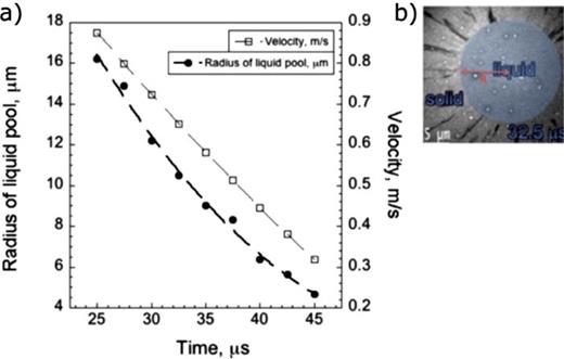
(a) Change in melt pool radius and solidification front velocity with time for pure Al. (b) BF 15-ns single-shot DTEM image used to determine the interfacial velocity after 32.5 μs, illustrating measurement of the melt-pool radius. Reproduced with permission from Kulovits et al., Philos. Mag. Lett. 91(4), 287–296 (2011). Copyright 2011 Taylor & Francis.
(a) Change in melt pool radius and solidification front velocity with time for pure Al. (b) BF 15-ns single-shot DTEM image used to determine the interfacial velocity after 32.5 μs, illustrating measurement of the melt-pool radius. Reproduced with permission from Kulovits et al., Philos. Mag. Lett. 91(4), 287–296 (2011). Copyright 2011 Taylor & Francis.
The data obtained on the morphology of the solid-liquid interface and kinetics of rapid solidification in this geometrically well-defined pure metal thin film system77 demonstrated the capability of the in situ DTEM technique to study more complicated alloy systems, where a solid grows into a supercooled rather than superheated liquid. These types of experiments can provide previously inaccessible information, suitable to assist in validation and improvement of predictive models for rapid solidification.68,82–87
2. Rapid solidification of a hypoeutectic Al-Cu alloy
Prior studies of rapid solidification have shown particular interest in Al-Cu alloys with Al-rich compositions due to the large body of well-defined thermophysical, optical, and solidification data that exists for this system.79,88–90 The Al-rich portion of the Al-Cu equilibrium phase diagram91 contains a eutectic with terminal phases of α-Al solid solution and the ordered intermetallic θ-Al2Cu phase. Numerous studies on the rapid solidification of Al-Cu alloys70–72,92–100 have reported observations of various microstructural features, including degenerate eutectics,70,93,99 cellular and dendritic morphologies,70,72,94,95,99 and banded structures.70,71,93,95,96,99 Solidification microstructure selection maps have been determined as a function of composition and solidification velocity70,99 for Al-rich Al-Cu alloys that were rapidly solidified after surface melting with a scanned continuous-wave laser. Furthermore, a solidification-front-velocity dependent extension of the range for eutectic growth has been established using Al-rich Al-Cu alloys as a model system and was rationalized in terms of a competitive growth model.101
Hypoeutectic alloys with composition Al-7 at. %Cu were pulsed-laser melted and the microstructural evolution during subsequent rapid solidification was monitored in situ in the DTEM.78 Figure 7 presents selections BF 15-ns single-shot DTEM images for two separate time-delay series. For each micrograph, the time delay after the laser pulse initiated melting of the alloy is shown as an inset. Scale markers are different for the two separate series of experiments and are shown for the first images in each series of Figures 7(a) and 7(b), respectively. The two time-resolved series were recorded at different magnifications to reveal various features of the microstructure evolution during rapid solidification.
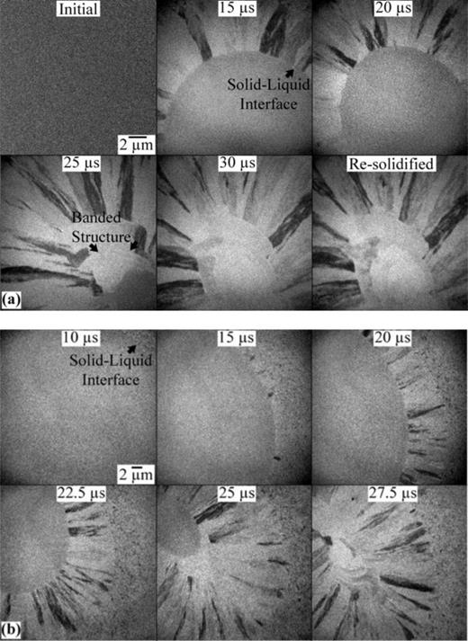
BF 15-ns single-shot DTEM images recorded before and at multiple time delays after laser melting of an Al-7 at. %Cu alloy. Scale bars in upper left apply to all images in (a) and (b), respectively. Images in (a) and (b) were recorded at different magnifications to capture various features of the microstructure during solidification. Reprinted with permission from McKeown et al., Acta Mater. 65, 56–68 (2014). Copyright 2014 Elsevier.
BF 15-ns single-shot DTEM images recorded before and at multiple time delays after laser melting of an Al-7 at. %Cu alloy. Scale bars in upper left apply to all images in (a) and (b), respectively. Images in (a) and (b) were recorded at different magnifications to capture various features of the microstructure during solidification. Reprinted with permission from McKeown et al., Acta Mater. 65, 56–68 (2014). Copyright 2014 Elsevier.
Prior to melting, the film showed little contrast at this magnification due to the fine-scale grain size, as shown in the first frame of Figure 7(a). The solid-liquid interface is indicated in the 15 μs and 10 μs images of Figures 7(a) and 7(b), respectively. The liquid melt pool appears featureless and lacks contrast, while the newly formed solid phase consuming the alloy melt displays contrast features in the BF DTEM micrographs as a result of grain growth and crystallographic orientation.
Prominent features of the solidification process are evident upon inspection of the time-resolved images of Figure 7. As in the case of pure Al, the solid-liquid interface was curved on the micron length scale (the melt pool was elliptical due to the angle between the laser and specimen, with dimensions of ∼27 μm and 35 μm for the minor and major axes, respectively), but appears morphologically smooth at length scales on the order of the film thickness (80 nm), with no evidence of dendritic growth at the solidification front. At a delay time between 20 and 25 μs, there was a marked change in the curvature of the solid-liquid interface to a more faceted, chevron-like appearance, which is apparent in the 25 μs images of both Figures 7(a) and 3(b). This change in the morphology of the interface was accompanied by a sudden increase in the velocity of the solidification front, seen by the noticeable decrease in the size of the melt pool. The morphology and velocity changes coincide with the onset of a large, central microstructural zone. This central zone consists of a banded structure (most clearly seen in the 25 μs image of Figure 7(a), as indicated) common to many rapidly solidified alloys71,102–105 when the solidification conditions approach a critical velocity leading to an instability106,107 at the solid-liquid interface. Finally, the alloy was completely re-solidified by ∼30 μs after the laser-induced melting of the alloy film.
Even at the relatively low resolution of the micrographs in Figure 7, it is apparent that morphologically distinct microstructural zones formed during rapid solidification. Around the periphery of the initial melt pool, a region of small grains with random orientations developed. This perimeter region of small, morphologically equiaxed grains generated a characteristic columnar zone, with columnar grains growing into the melt pool opposite to the direction of heat flow. The columnar zone abruptly terminated at a large, central microstructural zone consisting of what appears to be a few large grains with a complex intragranular banded structure.
Figure 8(a) shows a montage of BF TEM images that display the resultant microstructure of the rapid solidification process across an entire pulsed-laser-melted region. The solidified microstructural zones are evident, as labeled in Figure 8(a): (1) a heat-affected zone containing the small-grained morphology at the perimeter of the melt pool, (2) a transition zone, and (3) a growth zone containing the columnar morphology and large central grains. The contrast in the images of Figure 8(a) suggests that certain columnar grains forming zone 3 generated the complex central structure. Thus, the arrowed columnar grain on the right side of Figure 8(a) exhibits dark contrast after positioning the grain into a [011] zone-axis orientation, and it is clear that the large banded central structure and columnar structure are continuous and of identical orientation, i.e., they are part of the same grain. Notably, on the left side of Figure 8(a), the arrowed, strongly diffracting columnar grain wraps around another large banded grain in the central region of the microstructure. The two arrowed grains that partly constitute the central zone of the rapidly solidified alloy microstructure are not a single grain, but are separated by a grain boundary.
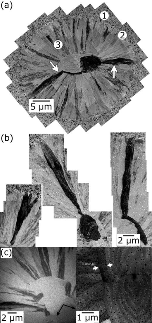
(a) Montage of conventional BF TEM images showing three distinct morphological zones in the re-solidified alloy film: (1) heat-affected zone containing a hypoeutectic structure, (2) a transition zone, and (3) a growth zone. (b) BF TEM montage images of three types of columnar grains in the re-solidified alloy. Each grain has been tilted into a zone-axis orientation for image acquisition. (c) BF 15-ns DTEM image (left) showing formation of the banded structure and a HAADF STEM image (right) showing the solidified banded structure. The white arrows indicate a “wraparound” columnar grain, showing that these grains are also banded. Reprinted with permission from McKeown et al., Acta Mater. 65, 56–68 (2014). Copyright 2014 Elsevier.
(a) Montage of conventional BF TEM images showing three distinct morphological zones in the re-solidified alloy film: (1) heat-affected zone containing a hypoeutectic structure, (2) a transition zone, and (3) a growth zone. (b) BF TEM montage images of three types of columnar grains in the re-solidified alloy. Each grain has been tilted into a zone-axis orientation for image acquisition. (c) BF 15-ns DTEM image (left) showing formation of the banded structure and a HAADF STEM image (right) showing the solidified banded structure. The white arrows indicate a “wraparound” columnar grain, showing that these grains are also banded. Reprinted with permission from McKeown et al., Acta Mater. 65, 56–68 (2014). Copyright 2014 Elsevier.
Zone 1 was found to consist of equiaxed proeutectic α-phase grains surrounded by a Cu-enriched phase at the grain boundaries.78 This results from the relatively soft profile of the incident Gaussian laser pulse used to heat the alloy film, leading to a mixed-phase (α + L) region around the perimeter of the melt pool where coarsening and pronounce phase separation can occur. Zone 2 is a transition zone, where grains of α-Al solid solution crystallize and grow inward toward the center of the melt pool. This growth commenced, based on the time-resolved images, ∼10 μs after melting with the pulsed laser. The α-Al solid solution grains grow with shapes elongated along the direction of growth opposite the direction of heat flow, deviating significantly from the equiaxed grain shapes in zone 1. The solidification front undergoes growth-mode changes in zone 2 and rapidly transitions to a columnar structure with a eutectic growth mode. This columnar morphology can reach an optimum growth form by an occlusion process, where competitive growth of these grains in zone 2 resulted in a subset of these grains expanding laterally sufficiently rapidly to obstruct growth of some neighboring grains. The grains surviving the occlusion process continued to grow inward toward the center of the melt pool, producing the morphologically columnar microstructure of zone 3.
The morphologically columnar grains of eutectic solidification product form the majority of the zone 3 microstructure. These large, elongated grains stretch from the edge of the melt pool (zone 2) to the central banded structure of zone 3, and they range in length from ∼10 to 15 μm and width from ∼0.5 to 2 μm with a thickness of 0.08 μm. Typically, between six to eight of the morphologically columnar eutectic grains of zone 3 are involved in another growth mode transition, which is associated with formation of the central banded solidification microstructure. Figure 8(b) shows BF TEM montage images of multiple grains that constitute the columnar morphology of zone 3. Each of these columnar grains was tilted to a strongly diffracting zone-axis orientation and therefore appears dark in contrast. Three types of columnar grains are shown in Figure 8(b): (left) grains that terminate at or before the central banded structure; (center) and (right) grains that form the central banded structure. The majority of columnar grains in zone 3 terminate at the central banded structure. The occlusion process continues in zone 3, which is particularly evident in the image showing the terminated columnar grains (left image in Figure 8(b)), where three grains are in a zone-axis orientation. Two of these grains are occluded by neighboring grains while one columnar grain terminates at the central banded structure. The central morphological region of zone 3 is comprised of grains that develop into large banded grains (center in Figure 8(b)) and those that wrap around these grains (right in Figure 8(b)). In all solidification experiments involving Al-7 at. %Cu alloys, only two large central banded grains developed, both along the major axis of the elliptical melt pool at the two points of highest curvature on the solid-liquid interface (see Figure 7). These grains are large in area, spanning ∼15 grain diameters along the solid-liquid interface. A number of “wraparound” grains form, growing along isotherms in the melt pool and wrapping around the central grains. This growth morphology is directly related to the solidification front velocity and an instability at the solid-liquid interface.
The central grains of zone 3 exhibit a morphologically banded internal microstructure, as shown in the BF DTEM and high angle annular dark field (HAADF) STEM images of Figure 8(c). This banded structure consists of alternating light and dark bands, as observed in prior studies,70,71,105 where the light bands are microsegregation-free α-Al, a product of partitionless crystal growth, and the dark bands are composed of the same eutectic micro-constituent that is present throughout the columnar structure. The arrows in Figure 8(c) delineate a “wraparound” grain, which also exhibits the banded morphology. This banding occurred perpendicular to the direction of heat flow (and temperature gradient) in both types of grains that constitute the central grains of zone 3. The first band that appeared in all of the rapidly solidified films is always the light contrast, microsegregation-free band. The overall arrangement of the alternating bands of partitionless and eutectic solidification product in the central structure appears to follow the profile of isotherms within the elliptical melt pool. The time-resolved BF TEM images from the DTEM time-delay series shown in Figure 7 provide direct evidence for the increase in crystal growth rate associated with the change in growth mode in zone 3 that produces the central banded morphology, and its growth is shown in Figure 8(c).
The solidification front velocities along the semi-major, a, and semi-minor, b, axes of the elliptical melt pool, and , have been determined and are shown in Figure 9. The solidification front velocities were determined by measuring the position of the solid-liquid interface with time, and , relative to the initial position, and , from the time-resolved TEM images, yielding functions for the position of the solid-liquid interface with time along the two axes.78 Evaluating the derivatives of these functions at each time, t, gave the instantaneous velocities of the solidification front, and , along the semi-major and semi-minor axes of the melt pool. Error bars were calculated by considering two additive effects: motion blur and the shot-to-shot fluctuation in the energy of the laser used to melt the alloy films.
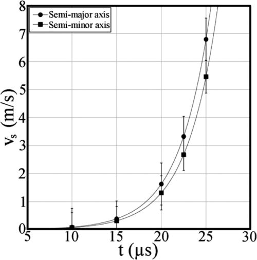
Plot of the velocity of the solidification front with time along the semi-major and semi-minor axes of the elliptical melt pool, as indicated, for the hypoeutectic Al-7 at. %Cu alloy, showing that the solid-liquid interface is accelerating. Reprinted with permission from McKeown et al., Acta Mater. 65, 56–68 (2014). Copyright 2014 Elsevier.
Plot of the velocity of the solidification front with time along the semi-major and semi-minor axes of the elliptical melt pool, as indicated, for the hypoeutectic Al-7 at. %Cu alloy, showing that the solid-liquid interface is accelerating. Reprinted with permission from McKeown et al., Acta Mater. 65, 56–68 (2014). Copyright 2014 Elsevier.
The varying curvature along the solid-liquid interface results in a range of solidification front velocities, with the maximum and minimum velocities occurring, respectively, along the semi-major and semi-minor axes of the melt pool, as these points of the solidification front exhibit the highest and lowest curvatures, respectively. The velocity for the time interval up to 20 μs corresponds entirely to the columnar eutectic product formation in zone 3 and was associated with increasing velocities up to ∼1.5 m/s, where the transition in growth mode to the central banded morphology was observed in the DTEM experiments at ∼20–25 μs delay time after pulsed-laser melting of the alloy. On average, the solidification front accelerated during the rapid solidification of the hypoeutectic Al-7 at. %Cu alloy, reaching a maximum velocity at the points of highest curvature (along the semi-major axis of the melt pool) of the transformation interface. These points of maximum velocity were the points of origin for the two large grains associated with formation of the vast majority of the central banded morphology (the instability at the solid-liquid interface initiated at these two points).
Rapid solidification experiments conducted with single-shot DTEM capabilities allowed in-situ observations of the evolution of the growth front morphology and quantification of solidification velocities with unprecedented spatial and temporal resolutions.78 The observed microstructural zones were related to the changes in velocity of the solidification front and crystal growth-mode transitions during solidification. The ability to capture growth-mode changes in situ during rapid solidification still remains somewhat challenging due to the accelerations associated with instability development and evolution. Finer temporal spacing between the images in a given series would allow observation with the required increased resolution in time to reveal additional mechanistic details of the crystal growth-mode transitions observed here during rapid solidification. Movie Mode DTEM experiments will allow multiple-image acquisitions from a single rapid solidification event, and future rapid solidification work will focus on these types of experiments with finer temporal resolution.
C. Morphological instabilities
Morphological instabilities during phase transformations can lead to distinct microstructures, as in formation of the banded structures observed during rapid solidification in Al-Cu alloys.70,71,78,105,106 Understanding the mechanisms of these instabilities can lead to improved control of the resultant microstructures and potentially unique properties, particularly in nanoscale material systems in which 2D and 3D arrangements of nanostructures can provide enhanced functionality at reduced cost and higher efficiency.108,109
1. Pulsed-laser dewetting of thin films
Pulsed-laser-induced dewetting of initially continuous ultrathin metal films has proven110–123 to effectively self-assemble metallic nanoparticle ensembles on substrates if the mechanisms and instabilities that control these processes can be understood. Generating arrays of nanoparticles with controlled size and spatial distributions is a key to the assembly of these ensembles, and processes that exploit morphological instabilities offer potential to attain fine-scale spatially correlated structures. There has been long-standing interest in capillarity and surface tension effects on morphological evolution in materials systems, dating back to the work of Plateau124 and Rayleigh.125 Multiple dewetting mechanisms can result from morphological instability in thin liquid films on substrates, leading to breakup of the films. Heterogeneous nucleation and growth of holes can initiate at defects in both the film and substrate.110,126–128 These nucleation events are typically random, unless a templated substrate is used to induce correlated heterogeneous nucleation. Spontaneous dewetting and formation of self-organized patterns with characteristic length scales can occur as a result of a competition between long-range dispersion or van der Waals forces and short-range surface tension forces.110,126,127,129–134 The magnitude of the dispersion force is dependent on the Hamaker coefficient, A,135–138 which describes the film-substrate interaction. For substrate/thin film/ambient systems, the film thickness will be unstable to surface perturbations when the magnitude of the dispersion forces overcome the stabilizing influence of surface tension, leading to morphological instability and spinodal dewetting. The spinodal dewetting of thin liquid metal films has been studied in detail110,113,139–145 and is typically the dominant mechanism for thin liquid metal films with thicknesses below tens of nanometers.
The liquid-phase dewetting dynamics of metallic thin films have been largely inferred by ex-situ observations of the re-solidified metal quenched after different liquid lifetimes,134 as thin-film metal dewetting uniquely has nanoscale length and timescales due to low viscosity and high surface energy. Herminghaus et al.110 used in-situ optical reflectometry to measure liquid lifetimes in pulsed-laser irradiated Au films, and several other studies111,142–144 have calculated time-temperature profiles and liquid lifetimes using both analytical and finite element or differencing models. To gain further insight to the dewetting and assembly dynamics, in-situ single-shot DTEM imaging and diffraction studies were conducted using ultrathin Ni films on silicon nitride support membranes.123
Figure 10 shows single-shot DTEM images of a 10-nm-thick Ni film region at multiple time delays after exposure to a pulsed laser with a total deposited energy of 4.1 μJ. The DTEM time labels for images and diffraction patterns are the delays between the arrival times of the peaks of the specimen heating laser pulse and the electron probe pulse at the specimen. Both pulse widths were ∼15 ns, and thus, each exposure (time-resolved diffraction pattern or image) was a time-averaged snapshot over 15 ns. Thus, for |t| < 10 ns, the two pulses overlap such that the sample was being rapidly heated during the electron exposure. Furthermore, each image represents a different area of the deposited film that was laser heated and imaged under identical experimental conditions but at different time delays; thus, some pulse-to-pulse variability is anticipated. For the images in Figure 10, the lower left corners of the images are approximately the center of the Gaussian laser pulse.
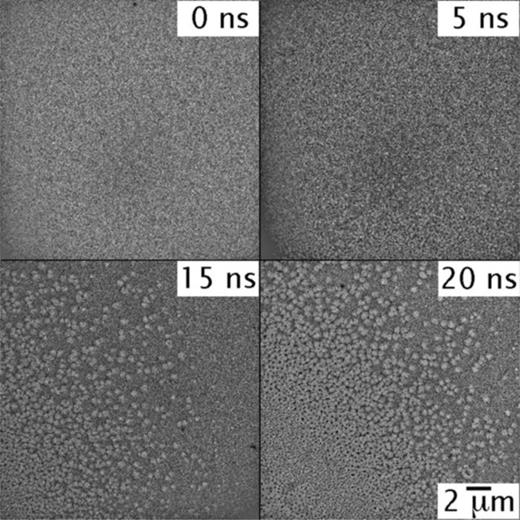
Single-shot 15-ns DTEM time-delay sequence of images as a 10-nm-thick nickel film dewets an amorphous silicon nitride substrate, after filtering and brightness and contrast equalization. Reprinted with permission from McKeown et al., Langmuir 28, 17168–17175 (2012). Copyright 2012 American Chemical Society.
Single-shot 15-ns DTEM time-delay sequence of images as a 10-nm-thick nickel film dewets an amorphous silicon nitride substrate, after filtering and brightness and contrast equalization. Reprinted with permission from McKeown et al., Langmuir 28, 17168–17175 (2012). Copyright 2012 American Chemical Society.
The observed liquid-phase nickel nanoparticle self-assembly process was attributed to a spinodal dewetting process. The 0 and 5 ns images do not show any hole or particle formation. The 15 ns image reveals saturated nanoparticles in the center ∼5 μm radius and progressive hole formation at larger radius. The 20 ns image nicely shows that the saturated nanoparticles extend to ∼10 μm and the hole formation extends to larger radius. Thus, the radial profile of the images also provides interesting temporal information: the film melted first in the center and there is a progressive delay in melting as a function of radius, as captured by the images in Figure 10. This was found to be consistent with thermal simulations.123
To determine whether the spinodal mechanism was the appropriate mechanism observed in this experimental regime, a series of films were deposited with varying thickness (h0 = 4, 6, 8, and 10 nm) and each was exposed to a single laser pulse at the same 4.1 μJ energy. Subsequent to irradiating the films, the nanoparticle distributions were imaged as a function of thickness and laser beam radius. Figure 11(a) shows a series of TEM images of the central laser spot region for different thicknesses, and Figure 11(b) is a plot of the most common nanoparticle spacing at the center region of the irradiated area based on a spatial correlation function (SCF) analysis versus film thickness. Following the procedure and disjoining pressure model, including both short- and long-range forces, outlined in Wu et al.,122 Figure 11(b) also shows the best fit (rms error ∼ 13 nm) of the particle spacing versus film thickness data, which yields an effective Hamaker constant of 3.8 × 10⁻¹⁸ J for the Van der Waals interaction of the liquid Ni surface and solid silicon nitride film. This value is the same order of magnitude as other experimentally determined liquid metal–solid Hamaker values.120,139,144,146 Assuming that the peak in the SCF is proportional to the wavelength of maximum growth (λm), we can estimate the maximum perturbation growth rate (σm) by122
where γ is the liquid surface energy (∼1.7 J/m2 (Ref. 147)) and μ is the liquid viscosity (4.76 × 10⁻³ Pa·s (Ref. 148)). Furthermore, the spinodal instability timescale is simply τm = 1/σm. Figure 11(b) also shows the consequent spinodal timescale as a function of original film thickness on the right y-axis. For a Ni film with initial thickness of 10 nm, the spinodal timescale was ∼25 ns.
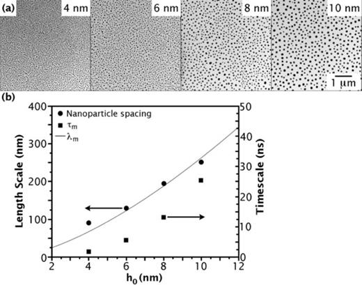
(a) BF TEM images of the resultant nickel nanoparticle distributions after a single 15-ns, 4.1-μJ pulsed laser exposure. The initial film thickness is noted in the upper right-hand corner. (b) Plot of the measured correlated nanoparticle spacing versus film thickness (circle data points) and the best fit of the data (thin line) for the effective Hamaker constant of 3.8 × 10⁻¹⁸ J. Also plotted on the right y-axis (square data points) is τm for the maximum spinodal instability timescale as a function of thickness. Reprinted with permission from McKeown et al., Langmuir 28, 17168–17175 (2012). Copyright 2012 American Chemical Society.
(a) BF TEM images of the resultant nickel nanoparticle distributions after a single 15-ns, 4.1-μJ pulsed laser exposure. The initial film thickness is noted in the upper right-hand corner. (b) Plot of the measured correlated nanoparticle spacing versus film thickness (circle data points) and the best fit of the data (thin line) for the effective Hamaker constant of 3.8 × 10⁻¹⁸ J. Also plotted on the right y-axis (square data points) is τm for the maximum spinodal instability timescale as a function of thickness. Reprinted with permission from McKeown et al., Langmuir 28, 17168–17175 (2012). Copyright 2012 American Chemical Society.
Time-resolved selected-area diffraction (SAD) patterns were also recorded as a function of time to complement the dynamic real-space imaging and estimate the Ni liquid lifetime. Figure 12(a) shows a series of SAD patterns taken at various delay times relative to the specimen heating laser's interaction with the specimen (including as-deposited and post-laser-pulse diffraction patterns using a long exposure time relative to that of the time-resolved diffraction experiments). The simulated diffraction pattern for polycrystalline nickel is included in the long-exposure as-deposited diffraction pattern. The conventional diffraction pattern from the as-deposited film shows broad diffraction rings due to finite crystal-size effects, indicating that the film is nanocrystalline, which is consistent with BF TEM images of the as-deposited film. After the film has dewet, the diffraction pattern shows spotted rings due to the larger-grain polycrystalline morphology.
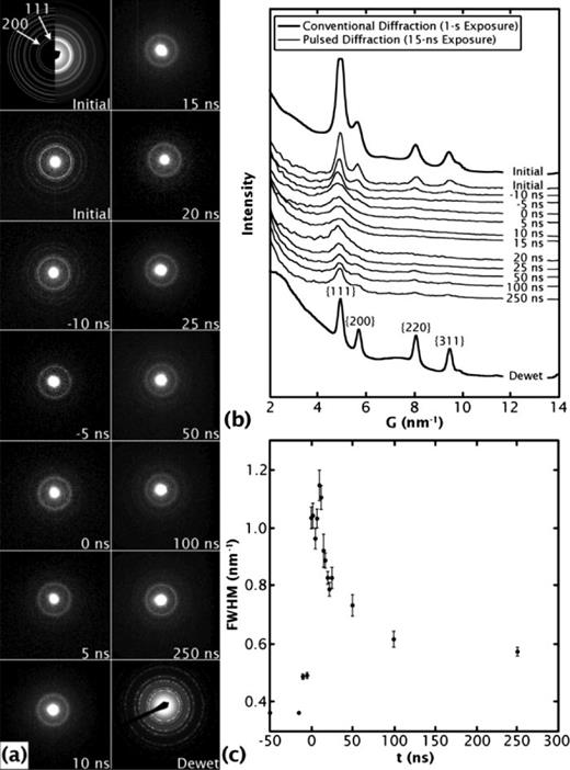
(a) Single-shot time-delay series of diffraction patterns showing the evolution of the Ni film as it dewets the substrate. The initial diffraction pattern recorded from the as-deposited film shows the simulated polycrystalline Ni diffraction pattern with the experimental pattern, recorded with a 1-s exposure time. The time evolution was followed in 5-ns intervals using 15-ns exposure times. (b) Radially averaged intensity as a function of reciprocal lattice vector, G, for all diffraction patterns shown in (a). (c) A plot of the FWHM of the peak centered around the {111} peak position (4.92 nm−1) as a function of delay time between the specimen heating laser and electron imaging pulse. Reprinted with permission from McKeown et al., Langmuir 28, 17168–17175 (2012). Copyright 2012 American Chemical Society.
(a) Single-shot time-delay series of diffraction patterns showing the evolution of the Ni film as it dewets the substrate. The initial diffraction pattern recorded from the as-deposited film shows the simulated polycrystalline Ni diffraction pattern with the experimental pattern, recorded with a 1-s exposure time. The time evolution was followed in 5-ns intervals using 15-ns exposure times. (b) Radially averaged intensity as a function of reciprocal lattice vector, G, for all diffraction patterns shown in (a). (c) A plot of the FWHM of the peak centered around the {111} peak position (4.92 nm−1) as a function of delay time between the specimen heating laser and electron imaging pulse. Reprinted with permission from McKeown et al., Langmuir 28, 17168–17175 (2012). Copyright 2012 American Chemical Society.
Inspection of the time-resolved diffraction patterns in Figure 12(a) reveals changes in the structure of the nickel film indicative of melting and re-solidification.149 There is a noticeable change in the short-range order at times as short as the first 10 ns (−5 ns diffraction pattern) after interaction of the laser with the specimen, evidenced by a broadening of the {111} diffraction ring and a disappearance of higher-index diffraction rings. Figure 12(b) shows radially averaged patterns of the experimental data in Figure 12(a) that more clearly illustrate the dynamics of the laser melting process. Following the progression of the peaks centered about the {111} and {200} lattice spacings, a broadening of both peaks is observed beginning at around −5 ns. The {111} peak continues to broaden and becomes diffuse with time, while the intensity of the {200} peak decreases with time, disappearing altogether by 5 ns, at which time the diffraction pattern consists of a single diffuse diffraction ring that is characteristic of a liquid, indicating that the region of the film from which the diffraction pattern was obtained is completely melted. Intensity in the {200} peak begins to return at ∼25 ns. This broadening of the {111} diffraction feature (4.92 nm−1) is shown in Figure 12(c), which plots the FWHM of the {111} peak as a function of time. The FWHM values were obtained by subtracting the background from the radially averaged patterns and fitting the {111} peak to a Lorentzian profile. The initial FWHM of the {111} peak in the as-deposited film is 0.36 nm−1 and reaches a maximum of 1.15 nm−1 at 10 ns, after which it begins to decrease as the film re-solidifies. The diffraction data and analysis in Figure 12 indicate a liquid lifetime of ∼20 ns (±7.5 ns half width of the electron beam pulse width).
In conclusion, ultrathin Ni films were found to dewet silicon nitride substrates by a spinodal mechanism. The spinodal timescale (∼25 ns) of the 10-nm-thick film determined by the thickness-dependent correlated nanoparticle spacing was consistent with the experimentally determined liquid lifetime from time-resolved diffraction patterns, DTEM imaging of the dewetting process, and finite difference simulations.123
D. Crystallization of amorphous elemental semiconductors
Electron and laser crystallization of amorphous semiconductor thin films is an important processing path for materials for optoelectronic devices. Devitrification of amorphous semiconductors has been studied by various techniques, including techniques with high temporal resolution, such as optical reflectivity and transmission experiments, but the high-spatial and temporal resolution of pulsed TEM provides a means to characterize both the microstructural evolution and transformation kinetics of highly driven phase transformations, revealing aspects of the thin-film devitrification that are inaccessible with other characterization techniques. Pulsed TEM with nanosecond-scale temporal resolution has been used to study electron-pulse-induced crystallization of amorphous Sb150 and both electron- and laser-induced crystallization of Si,22,151,152 and Ge.22–24,29,31,153–156
1. Crystallization of amorphous antimony
The first application of pulsed TEM to the study of the crystallization of amorphous semiconductors was Bostanjoglo and Schlotzhauer's work on electron-pulse crystallization of amorphous Sb films.150 Amorphous Sb films were locally heated with 20–50 μs electron pulses. Crystallization started at the center of the electron beam irradiated area and spread in a self-sustaining exothermic transformation beyond the illuminated region, crystallizing the entire Sb film. The crystallization front velocity and the texture of the final phase in the electron beam illuminated areas depended on the electron beam current density. For pulsed electron current densities <0.02 A/mm2, a mosaic crystalline microstructure formed in both the irradiated and un-irradiated areas. For current densities (>0.1 A/mm2), large (>1 μm) single crystals formed within the electron irradiated area and the rest of the film crystallized as a fine mosaic crystal. The phase transformation was not imaged, but the occurrence of crystallization was inferred by a change in BF image intensity in a region of the specimen delimited by a field-limiting aperture, tracked with a photomultiplier and storage oscilloscope with a temporal resolution of 3 ns. The crystallization front speed was approximated from the time it took the 0.5 μm diameter region defined by the aperture to transition from high bright-field intensity to a lower intensity. From this detection method, the mosaic crystal front was estimated to advanced at ∼2.5 m/s and single crystal front at ∼80 m/s.
2. Crystallization of amorphous silicon
Bostanjoglo22 used the same technique of tracking crystallization by a change in BF image intensity to study crystallization of amorphous Si thin films. Crystallization was initiated with a 50-μs electron pulse and the change in image intensity due to the growth of crystals in a 0.5 μm diameter region defined by a field-limiting aperture was detected (Figure 13). With this detection method, the crystallization rates could be approximated and growth rates in different areas of the electron pulse affected area were found to vary from roughly 0.05 m/s to potentially as high as ∼100 m/s.
Electron-pulse-crystallized Si. (a) The three microstructural zones after crystallization. (b) Rectangle of (a); the field of view of the multiplier is circled. (c) Bright-field image intensity of the circled area in (b) during the pulse showing the crystallization step (20 mV, 5 μs/div). Amorphous and crystalline phase intensities are labeled “a” and “cr.” (d) Crystallization step in (c)) at increased scale (20 mV, 10 ns/div). The area of crystal circled in (b) was formed in ∼5 ns. Reprinted with permission from O. Bostanjoglo, Phys. Status Solidi A 70(2), 473–481 (1982). Copyright 1982 John Wiley & Sons, Inc.
Electron-pulse-crystallized Si. (a) The three microstructural zones after crystallization. (b) Rectangle of (a); the field of view of the multiplier is circled. (c) Bright-field image intensity of the circled area in (b) during the pulse showing the crystallization step (20 mV, 5 μs/div). Amorphous and crystalline phase intensities are labeled “a” and “cr.” (d) Crystallization step in (c)) at increased scale (20 mV, 10 ns/div). The area of crystal circled in (b) was formed in ∼5 ns. Reprinted with permission from O. Bostanjoglo, Phys. Status Solidi A 70(2), 473–481 (1982). Copyright 1982 John Wiley & Sons, Inc.
Conventional TEM imaging after crystallization was used to characterize the complex microstructure cause by electron beam irradiation. The electron-beam crystallized regions generally consisted of up to three distinct regions, shown in Figure 13. If the electron pulse current is high enough, the central region, which was heated to the highest temperature, is polycrystalline and consists of nano-sized grains (zone I). The region surrounding zone I consists of elongated grains with major axes that are oriented radially (zone II). Zone II is often encircled by elongated grains with major axes that are oriented tangentially (zone III), spiraling around the central crystallized region. Zones II and III are separated by a feathery-appearing fine-grained structure, and the large tangentially oriented grains forming the spirals of zone III are similarly separated by a fine-grained structure. Similar three-zone microstructure occurs in electron- and laser-crystallized Si and Ge. The three zones of microstructure are complex compared to the relative straightforward crystallization of an intermetallic.157,158 In this review, the zone I–III terminology will be used for Si and Ge, where this three-zone microstructure develops. Bostanjoglo22 conjectured that the formation of the different zones was due to changes in temperature profile in the heat-affected area or due to changes in impurity profile as the crystallizing material rejected impurities, however, an analysis of the relationship between the temperature profile and zones was not performed, and no post-mortem analysis was performed to confirm the presence of compositional fluctuations, leaving this as an open question. The development of Zone II and III was investigated in more detail in amorphous Ge and will be discussed in Sec. IV D 3.
Laser-crystallization of amorphous Si was later studied by Kwon et al.151 using single-pulse electron diffraction with 15-ns resolution. Single-pulse diffraction patterns were taken during different stages of the crystallization of amorphous Si, by repeating with single-pulse experiment for different time delays (relative to the crystallizing laser pulse) on fresh areas of amorphous Si. With increased time, the diffraction pattern changed from broad rings of the amorphous Si to well-defined diffraction rings from fine-grained crystalline Si. Time-resolved diffraction profiles were constructed by radially averaging diffraction patterns and normalizing to total electron count for each delay. Each diffraction profile was fitted with a linear combination of profiles from completely amorphous and completely crystalline Si. The percent contribution of crystalline pattern to the fitted profile was taken as a measure of the degree of crystallization at each time delay. From this analysis, they obtained a characteristic time of 880 ± 140 ns for the final transformation. Since no field-limiting aperture was used, the signal came from a large area of the specimen, and the temporal development represents a spatially averaged view of the amorphous-to-crystalline transition over a large area of the specimen.
Taheri et al.152 performed single-shot DTEM imaging during the laser-crystallization of Si to observe melt-mediated crystallization of amorphous Si. Amorphous Si on a thin SiO2 support was heated with a 532 nm laser light with a fluence (155 mJ/cm2) where the amorphous Si was assumed to melt, just below the threshold where dewetting from the SiO2 was observed. Given the thin electron transparent specimen geometry, it was estimated that, once the amorphous Si melted, hundreds of nanoseconds were required to cool below the melt temperature. A 15-ns image, taken 100 ns after the laser pulse struck the specimen, showed bubbles forming in the Si, taken as evidence of its molten state. After a 300 ns delay, fine-grained material was visible at the edge of the laser irradiation zone. Based on these observations, it was hypothesized that the fine-grained material formed via solid-state crystallization and those grains provide sites for rapid solidification of large crystals into the hot liquid zone at the center of the laser-irradiated area.
3. Crystallization of amorphous germanium
Considerably more time-resolved TEM has been devoted to the study of the laser crystallization of amorphous Ge. Work performed at TU Berlin in the 1980s22–24 used the same method to detect crystallization as had been applied to Sb and Si: the occurrence of crystallization was inferred from changes in BF intensity from sub-micron regions of the specimen defined by a field-liming aperture. Both electron-pulse22,24 and laser-pulse crystallization23 of amorphous Ge were studied. The resulting crystallized microstructures were similar whether formed by electron- or laser-irradiation of the Ge and were similar to microstructures formed upon crystallization of Si, consisting of the three zones I, II, and III,22,24 described in Sec. IV D 2 (see Figure 14). Changes in the bright field intensity were detected with <4 ns resolution, and the initiation of crystallization was observed to occur within ∼5–10 ns of the pulse irradiation of the amorphous Ge. Crystal growth velocities were approximated for different areas of the irradiated Ge. The highest growth velocities (∼tens of m/s) were observed in the radial grains of zone II. Growth velocities in zones I and III were considerably lower.22,23 Bostanjoglo and Endruschat23 proposed that the observed high growth velocities and other details of the microstructural development could be explained by the amorphous melting, i.e., melting of an amorphous phase, which may occur considerable below the crystalline melting temperature, resulting in a supercooled liquid.
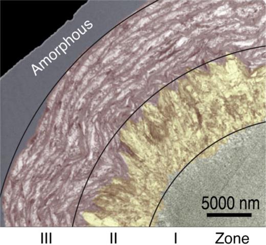
Conventional bright-field TEM image of a laser crystallized area in 110 nm thick a-Ge. The three microstructural zones (I–III) are labeled. False color added to accentuate zones. Reprinted with permission from Nikolova et al., Phys. Rev. B 87(6), 064105 (2013). Copyright 2013 American Physical Society.
Conventional bright-field TEM image of a laser crystallized area in 110 nm thick a-Ge. The three microstructural zones (I–III) are labeled. False color added to accentuate zones. Reprinted with permission from Nikolova et al., Phys. Rev. B 87(6), 064105 (2013). Copyright 2013 American Physical Society.
As the instrumentation at TU Berlin was developed, Bostanjoglo et al.31 used single-shot thermionic pulsed TEM with exposure times of 10–20 ns to laser-induced crystallization in amorphous Ge films. The growth front in Zone II was estimated to be about 10 m/s, similar to what had been previously estimated from bright-field intensity measurements. Due to the high level of shot noise, the resolution did not exceed that of light microscopy, but the ability to image the developing microstructure on the nanosecond scale represented an advance in that intermediate stages of crystallization were imaged. The radial Zone II growth of crystals was seen to propagate by mostly flat phase boundary 100–600 ns after the initiating ∼0.1 μJ laser pulse.
The TU Berlin group subsequently used pulsed double-frame TEM29,154 with exposure time that could be varied between 10 and 50 ns and a delay time between two exposures that could as low as 100 ns to image laser-induced crystallization of amorphous Ge. With laser pulse power densities of 10–50 MW cm−2,29 holes formed at the center of the laser pulse. Images showed crystallization starting outside the hottest region ∼10 ns after the laser pulse and continuing for hundreds of nanoseconds, confirming the previous observations from the bright-field intensity measurements and single-shot TEM imaging.
Further experiments at TU Berlin explored the effect of different laser energies in the crystallization process.154 It was found that at high enough power densities, a fourth zone was observed to occur in the center of laser spots. At the center of the fine polycrystalline zone I region (which was believed to arise where the laser induced amorphous melting) was a region with larger grains. It was suggested that the specimen had been heated above the crystalline melting temperature, resulting in a lower nucleation rate. Crystallization was delayed by microseconds, presumably the time needed for the melt pool to supercool, then proceeded inward by growth of single-crystal grains with velocities ∼0.5 m/s. Though the imaging had low spatial resolution, it was adequate to distinguish the growth front of very large crystals and extract an estimated crystal growth front speed.
Laser crystallization of amorphous Ge was re-visited by Nikolova et al. using the single-shot pulsed photoemission DTEM at LLNL, which had significantly better spatial resolution compared to the pulsed thermionic emitter at TU Berlin.155 Time resolved imaging using 15-ns single shot DTEM could resolve crystalline grains once they grew to more than ∼40 nm. This resolution capability allowed the measurement of size of growing grains as a function of time and estimation of the nucleation rate for the sub-micron grains that developed in the Zone I region during laser crystallization. Near the center laser-heated region, where it was estimated the Ge reached ∼1100 K (above the reported melting temperature for amorphous Ge, but below the melting temperature of crystalline Ge), DTEM observations showed that supercritical nuclei are formed less than 20 ns after laser excitation and that complete crystallization in this local region could occur within ∼55 ns. From the number of crystals in each time-resolved image, the maximum nucleation rate was estimated to be ∼1.6 × 1022 cm−3 s−1. The time for zone I crystallization increases away from the center of the laser excitation spot, with zone I crystallization completing ∼275 ns after laser excitation for the laser fluences used.
Single-shot DTEM at LLNL was also used to study the microstructural development in zones II and III in detail.156 Grains at the outer edge of zone I provided initiation sites for growth of the large Zone II grains. The average growth velocity in the radial direction of Zone II was observed to be 8 ± 2 m/s. The growth front appeared relatively flat in the early stage of crystal growth in Zone II as observed by TU Berlin group, but at longer delays the Zone II crystallization front developed prominent protrusions (Figure 15). It was suggested the protrusions in the growth front resulted from a Mullins-Sekerka-type instability. Using a simple model, it was calculated that the interfacial temperature for a crystallization front growing at 8 m/s and with a dendritic tip radius of ∼1.7 μm radii to be 1130 K. This temperature exceeds published values for the melting temperature of amorphous Ge but is below the crystalline melt temperature. It was suggested that the dendritic instability and growth rate model indicated that crystallization in Zone II is not a direct amorphous-crystalline interface, but liquid phase crystallization with co-propagating solid-liquid and liquid-amorphous interfaces.
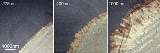
Time-resolved single-shot DTEM images of the formation of Zone II microstructure during crystallization of a-Ge. Large, radially elongated crystals grow from the Zone I boundary with a radial velocity of approximately 8 m/s. The initially flat crystallization front (275 ns) develops protrusions (400 ns) that have an increasingly faceted appearance (1000 ns). False color added to accentuate zones. Reprinted with permission from Nikolova et al., Phys. Rev. B 87(6), 064105 (2013). Copyright 2013 American Physical Society.
Time-resolved single-shot DTEM images of the formation of Zone II microstructure during crystallization of a-Ge. Large, radially elongated crystals grow from the Zone I boundary with a radial velocity of approximately 8 m/s. The initially flat crystallization front (275 ns) develops protrusions (400 ns) that have an increasingly faceted appearance (1000 ns). False color added to accentuate zones. Reprinted with permission from Nikolova et al., Phys. Rev. B 87(6), 064105 (2013). Copyright 2013 American Physical Society.
An abrupt transition from Zone II to Zone III growth was observed, where layers formed by grains growing tangentially to the outer edge of zone II, as in Figure 14. Zone III consisted of large elongated grains with feathery-looking nanocrystalline areas bounding the edges of the large grains. Single-shot DTEM images confirmed that the growth direction for zone III is perpendicular to the direction of macroscopic crystallization (and net heat flow). The primary growth direction for each tangentially elongated crystal is in the azimuthal direction and outward crystallization progresses by accumulation of additional interleaved layers. The radial growth velocity in zone III was estimated to be ∼1 m/s, approximately an order of magnitude lower than in zone II. After zone III development starts it may continue to grow for many microseconds.
To help understand the role of the temperature profile (both established by the laser and arising from the heat of crystallization) in the development of zones II and III, the time-evolving average radial temperature profile in the Ge film was calculated. The temperature profile was modeled as a 2D heat flow problem and included the heat evolved at the crystallization front. The calculations showed that, for the experimental geometry used, the average temperature at the crystallization front drops through zone II, approximately following the decline of the underlying Gaussian temperature profile created through laser heating. Once initiated, Zone II growth continues over several microns due to the exothermic character of the crystallization and the underlying Gaussian temperature profile. The calculations suggested that the abrupt change in the crystallization dynamics occurs once the temperature at the rapidly advancing Zone II front drops below the lower threshold for the rapid (liquid phase) crystallization. Zone III crystallization then occurs along narrow (∼1 μm) bands in the orthogonal direction where the crystallization front follows an approximately isothermal curve. This growth mode matches the radial advance of crystallization with thermal diffusion in the radial direction. The diffusion length in 1 μs is ∼6 μm, sufficient to prepare a narrow adjacent band of material to support growth of an additional layer. Crystallization stops when the temperature of the adjacent amorphous material drops below a critical level for crystallization. Comparison of crystallization times with thermal diffusion timescales suggested that crystal growth in zones II and III was driven by latent heat released at the crystallization interface and not purely by thermal diffusion of laser-deposited energy.
E. Reactive multilayer films
Reactive multilayer metal foils (RMMFs) consist of thin stacks of metals that undergo exothermic, self-propagating reactions when layer mixing is induced by an external energy source (Figure 16).159 High-temperature reaction zones develop in the region where interdiffusion and intermetallic phase formation occurs.160 The reaction zone temperature and reaction front velocity are controlled by composition and thickness of the individual multilayers. RMMFs are used as localized heat sources for fuses and joining of materials. They are also model systems for studying the effect of steep concentration gradients on the formation of intermetallic phases. The nanoscale geometry and rapid reaction front velocities limit the characterization methods capable of probing the phase transformations occurring in RMMFs, but single-shot DTEM has yielded both crystallographic and microstructural data from direct observations of self-propagating reaction fronts in Al-Ni RMMFs.159,161

Schematic of RMMF reaction-front where mixing is initiated locally by a laser. The reaction propagates in the foil until the elemental layers converted into an intermetallic by the mixing reaction. Reprinted with permission from Kim et al., Science 321(5895), 1472–1475 (2008). Copyright 2008 AAAS.
Schematic of RMMF reaction-front where mixing is initiated locally by a laser. The reaction propagates in the foil until the elemental layers converted into an intermetallic by the mixing reaction. Reprinted with permission from Kim et al., Science 321(5895), 1472–1475 (2008). Copyright 2008 AAAS.
Kim et al.159 used single-shot DTEM with 15-ns resolution in both diffraction and imaging modes to study the propagation and behavior of RMMFs consisting of five bilayers totaling 125 nm in thickness of Al:Ni0.91V0.09 at a 2:3 atomic ratio. Reactions were initiated with a 12-μJ, 3-ns laser pulse. The self-propagating reactions were imaged, revealing a transient cellular morphology at the reaction front (Figure 17). The reactions were imaged hundreds of microns from the laser initiation site where the reaction had reached a self-propagating state outside the laser-heated area. The size of the transient structures was far greater than the Al:Ni bilayer thickness leading to the conclusion that they were not an artifact of the deposited multilayer structure but a transverse structure in the film inherent to the reaction process. The cellular morphology of the reaction front was interpreted as lines of mass-thickness contrast due to phase formation of an ordered B2 NiAl phase and liquid. A brief phase separation was also observed during cooling. Single shot electron diffraction patterns with 15-ns-resolution were obtained for times before, during, and after the passing of the reaction front. The electron pulse was limited by the TEM condenser aperture and condensed to a 11.2 mm diameter spot on the sample, which was smaller than the width of the transient cellular structures observed in the DTEM images. The diffraction data showed the ordered B2 NiAl phase forms from the Al and Ni0.91V0.09 layers less than 300 ns after the arrival of the reaction front.
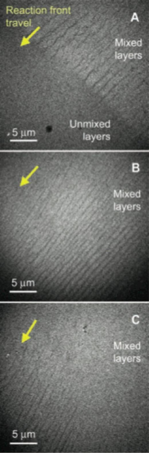
The propagation of a mixing front in a Al/Ni RMMF imaged in three 15-ns single-shot DTEM images. Image (a) shows the edge of the reaction front for defined delay after the specimen has been laser heated. The experiment is repeated (b) with 2 μs longer delay than in (a). With an even longer relative delay (5 μs longer relative to (a)) the layers have completed mixing in the center of image (c). The time-resolved images reveal a transient cellular structure that is only apparent during the reaction. Reprinted with permission from Kim et al., Science 321(5895), 1472–1475 (2008). Copyright 2008 AAAS.
The propagation of a mixing front in a Al/Ni RMMF imaged in three 15-ns single-shot DTEM images. Image (a) shows the edge of the reaction front for defined delay after the specimen has been laser heated. The experiment is repeated (b) with 2 μs longer delay than in (a). With an even longer relative delay (5 μs longer relative to (a)) the layers have completed mixing in the center of image (c). The time-resolved images reveal a transient cellular structure that is only apparent during the reaction. Reprinted with permission from Kim et al., Science 321(5895), 1472–1475 (2008). Copyright 2008 AAAS.
Further work by Kim et al.161 used single-shot DTEM to identify intermetallic products and phase morphologies during exothermic self-propagating reactions in RMMFs with overall atomic ratios of 3:2, 2:3, and 1:1 Al:Ni (with small additions of vanadium) after initiation with a laser pulse. Time-resolved imaging revealed a transient cellular morphology in the 3:2 and 2:3 Al:Ni foils, but not in the equiatomic films. The cellular features in the Al-rich and Ni-rich films were ascribed to the co-existence of solid NiAl and a liquid phase below the NiAl congruent melting temperature during the mixing reaction, which was absent in the 1:1 Al:Ni foils. The 15-ns time resolved diffraction data showed only the formation of the B2 NiAl intermetallic phase for all three Al:Ni ratios studied. The absence of detectable amounts of other intermetallic phases, such as Al3Ni2 or AlNi3, in the foils regardless of the overall composition differs from observations made in other studies using differential scanning calorimetry and x-ray diffraction, though it should be noted that post-mortem energy-dispersive X-ray spectroscopy (EDS) of the Al-rich films showed a significant loss of Al occurred during the reaction.
The recently developed simultaneous nanocalorimetry and DTEM technique60 have been applied to 1:1 Al:Ni bilayer RMMFs.162 Interfacial reactions of Al/Ni layers at heating rates below 1 K/s show that the phase transformation sequence starts with the most Al-rich phase and continues through progressively more Ni-rich phases. In the nanocalorimetry and DTEM experiments, single 100 nm Al/Ni bilayers were deposited onto nanocalorimeter sensors that could measure temperature and heat flow for heating rates up to 100 000 K/s. The sensors were loaded into the DTEM and heated at an average of 830 K/s while measuring the heat flow and acquiring pulsed electron diffraction patterns. Heat flow measurements showed a sequence of three exothermic peaks. The simultaneously captured diffraction patterns were used to identify the intermetallic phases present and reconstruct the phase transformation sequence as a function of time and temperature. The DTEM diffraction and nanocalorimetry showed that the transformation sequence when heating at 830 K/s is Al + Ni → Al3Ni + Ni → Al3Ni2 + Ni → AlNi, the same sequence that occurs at low heating rates.
F. Martensitic transformations
Martensitic transformations are an important class of solid-solid phase transformations that enabled the Industrial Revolution through the hardenability of steel.163 The transformation proceeds by a coordinated motion of atoms to assume a new crystal structure and is thought to propagate through a crystal at speeds approaching the speed of sound.164 However, the topology of the interface between the martensite phase and the austenite phase dictates that certain defects be present165,166 and in as much as the motion of these defects is limited by the speed of sound then interfacial motion may be significantly less than the speed of sound. The investigation of these interfaces in motion with the DTEM has led to limited success,167,168 essentially because they are still too fast for effective imaging even with 15 ns temporal resolution.
V. OUTLOOK
To date, time resolved electron microscopes have been the result of capability and technique development efforts within the labs of individual investigators and small groups of researchers. While these groups have had great success in applying the technique to interesting problems in materials science, the spread of the technique to a broader community has been slow. However, there recently has been introduced the availability of these systems from commercial vendors. This new availability to the microscopy community promises that the technique will receive more widespread application. Most of the systems installed to date have been based on the stroboscopic approach because of its less demanding technical requirements, and thus, the scientific fields impacted have been limited to those which this technique is suited. Now, with the single shot instrumentation available from a commercial source, we may expect a broader application of time resolved electron microscopy to the field of materials science, such as those reviewed here, and beyond to the life sciences.
VI. CONCLUSIONS
Time resolved electron microscopy has been evolving since the 1960s and showing steady progress in the improvement of spatial and temporal resolution. The single shot configuration has demonstrated particular usefulness for materials science studies. The materials science investigations typically involve dynamic processes that are irreversible (or lossy) in a thermodynamic sense, such as phase transformations or crystal defect motion. These processes do not unfold identically each time they proceed, and, in fact, it is these details of the differences that are interesting topics of study. Thus, single shot images of the evolution of individual events are more useful than ensemble averages yielded by the stroboscopic method. We have presented materials science investigations that produced novel results because the measurements made have been in regimes never before accessible.
ACKNOWLEDGMENTS
This work performed under the auspices of the U.S. Department of Energy, Office of Basic Energy Sciences, Division of Materials Sciences and Engineering for FWP SCW0974 by Lawrence Livermore National Laboratory under Contract No. DE-AC52-07NA27344.

